Build Stage Introduction
General
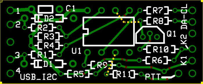
This kit will actually be built in a single stage, followed by a stage for setting up the interconnections to the rig(s) of choice.Build Stage Schematic
(Resistor testpoints (hairpin, top, or left-hand lead), as physically installed on the board, are marked in the schematic with red dots)
(Click for Full Schematic)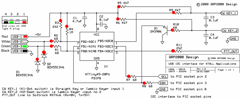
Build Stage Bill of Materials
Stage Bill of Materials
(resistor images and color codes courtesy of WIlfried, DL5SWB's R-Color Code program)
| Check | Designation | Component | Marking | Category | Orientation | Notes | Circuit |
|---|---|---|---|---|---|---|---|
| ❏ | D1 | BZX55C3V6 zener | BZX55C | Axial | flat-horiz | Build Stage | |
| ❏ | D2 | BZX55C3V6 zener | BZX55C | Axial | flat-horiz | Build Stage | |
| ❏ | R04 | 1 M 1/6W 5% | brn-blk-grn-gld
 | 1/6W | flat-horiz | Build Stage | |
| ❏ | C02 | 0.1 uF | (smt) black stripe
 | SMT 1206 | Build Stage | ||
| ❏ | C01 | 4.7 uF 10% | 475
 | Ceramic | Build Stage | ||
| ❏ | R01 | 68 1/6W 5% | bl-gry-blk-gld
 | 1/6W | flat-horiz | Build Stage | |
| ❏ | SO1 | 8 pin dip socket | socket | Build Stage | |||
| ❏ | C03 | 0.1 uF | (smt) black stripe
| SMT 1206 | Build Stage | ||
| ❏ | R03 | 2.2 k 1/6W 5% | r-r-r-gld
 | 1/6W | flat-horiz | Build Stage | |
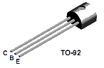
| ❏ | Q1 | 2N3906 PNP transistor | 2N3906
 | TO-92 | Build Stage | ||
| ❏ | C04 | 0.1 uF | (smt) black stripe
| SMT 1206 | Build Stage | ||
| ❏ | R02 | 68 1/6W 5% | bl-gry-blk-gld
| 1/6W | flat-horiz | Build Stage | |
| ❏ | R05 | 4.7 k 1/4 W 5% | y-v-r-gld
 | 1/4W | flat-horiz | Build Stage | |
| ❏ | R06 | 4.7 k 1/4 W 5% | y-v-r-gld
| 1/4W | flat-horiz | Build Stage | |
| ❏ | R07 | 68 1/6W 5% | bl-gry-blk-gld
| 1/6W | flat-horiz | Build Stage | |
| ❏ | R08 | 68 1/6W 5% | bl-gry-blk-gld
| 1/6W | flat-horiz | Build Stage | |
| ❏ | R09 | 4.7 k 1/4 W 5% | y-v-r-gld
| 1/4W | flat-horiz | Build Stage | |
| ❏ | R10 | 68 1/6W 5% | bl-gry-blk-gld
| 1/6W | flat-horiz | Build Stage | |
| ❏ | R11 | 2.2 k 1/6W 5% | r-r-r-gld
| 1/6W | flat-horiz | Build Stage |
Build Stage Summary Build Notes
- Mount SMT Caps
- Mount the Diodes
- Mount R1 and R3
- Mount R2 and R4
- Mount remaining resistors
- Mount C01, SO1, and Q1
- Test the Stage
Build Stage Detailed Build Notes
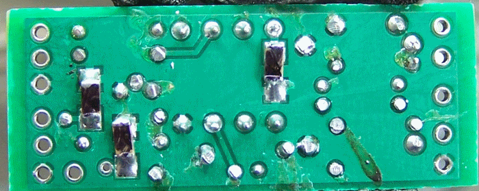
Bottom of the Board
Mount SMT Caps
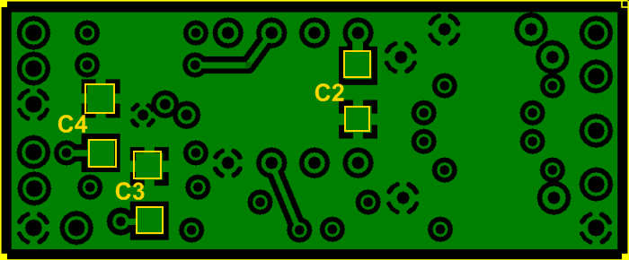
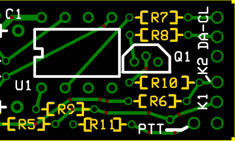
Mount SMT caps C02-C04 to the bottom side. Take care not to "launch" one off into space - you'll never find it. Tony has packed one extra in the kit, just for that contingency.
The image above shows the bottom-side location of the mounting pads for each of the 3 capacitors (highlighted in yellow)
| Check | Designation | Component | Marking | Category | Orientation | Notes |
|---|---|---|---|---|---|---|
| ❏ | C02 | 0.1 uF | (smt) black stripe
| SMT 1206 | ||
| ❏ | C03 | 0.1 uF | (smt) black stripe
| SMT 1206 | ||
| ❏ | C04 | 0.1 uF | (smt) black stripe
| SMT 1206 |
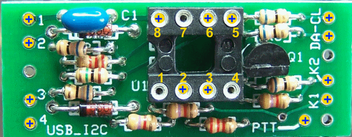
Top of the Board
Mount the Diodes
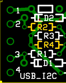
The two zeners are to protect the PC USB port, not the AVR chip, as that runs off a 5V supply. They are there with R1 and R3 to limit the USB signals to the PC to nominal level of 3.6v maximum.
Look very carefully at the photo of the top of the board. Depicted as faint yellow dashed lines are two traces from the bottom of the board which, together with the traces at the top, cover all the circuit traces. These are provided visually here should you have a need to trace signals on the board.
Space is quite constrained in the area of the diodes and resistors R1-R4. Components will have to be mounted in a sort of vertically "stacked" fashion in order to fit all of them in. See the photo below:
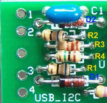
Mount D1 and D2, flush to the board. Banded end toward the left-hand edge of the board
| Check | Designation | Component | Marking | Category | Orientation | Notes |
|---|---|---|---|---|---|---|
| ❏ | D1 | BZX55C3V6 zener | BZX55C | Axial | flat-horiz | |
| ❏ | D2 | BZX55C3V6 zener | BZX55C | Axial | flat-horiz |
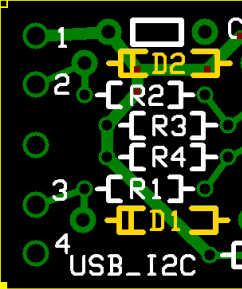
Mount R1 and R3
Mount R1 and R3 flush to the board
| Check | Designation | Component | Marking | Category | Orientation | Notes |
|---|---|---|---|---|---|---|
| ❏ | R01 | 68 1/6W 5% | bl-gry-blk-gld
| 1/6W | flat-horiz | |
| ❏ | R03 | 2.2 k 1/6W 5% | r-r-r-gld
| 1/6W | flat-horiz |
Mount R2 and R4
Mount R2 and R4, raised slightly above the board, to provide separation between resistor bodies.
| Check | Designation | Component | Marking | Category | Orientation | Notes |
|---|---|---|---|---|---|---|
| ❏ | R04 | 1 M 1/6W 5% | brn-blk-grn-gld
| 1/6W | flat-horiz | |
| ❏ | R02 | 68 1/6W 5% | bl-gry-blk-gld
| 1/6W | flat-horiz |
Mount remaining resistors
Mount remaining resistors flush to the board
| Check | Designation | Component | Marking | Category | Orientation | Notes |
|---|---|---|---|---|---|---|
| ❏ | R05 | 4.7 k 1/4 W 5% | y-v-r-gld
| 1/4W | flat-horiz | |
| ❏ | R06 | 4.7 k 1/4 W 5% | y-v-r-gld
| 1/4W | flat-horiz | |
| ❏ | R07 | 68 1/6W 5% | bl-gry-blk-gld
| 1/6W | flat-horiz | |
| ❏ | R08 | 68 1/6W 5% | bl-gry-blk-gld
| 1/6W | flat-horiz | |
| ❏ | R09 | 4.7 k 1/4 W 5% | y-v-r-gld
| 1/4W | flat-horiz | |
| ❏ | R10 | 68 1/6W 5% | bl-gry-blk-gld
| 1/6W | flat-horiz | |
| ❏ | R11 | 2.2 k 1/6W 5% | r-r-r-gld
| 1/6W | flat-horiz |
Mount C01, SO1, and Q1
Mount the ceramic cap, the socket for U1, and the 2n3906 transistor
| Check | Designation | Component | Marking | Category | Orientation | Notes |
|---|---|---|---|---|---|---|
| ❏ | C01 | 4.7 uF 10% | 475
| Ceramic | ||
| ❏ | SO1 | 8 pin dip socket | socket | |||
| ❏ | Q1 | 2N3906 PNP transistor | 2N3906
| TO-92 |
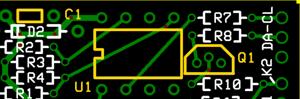
Build Stage Completed Stage
Top of the Board
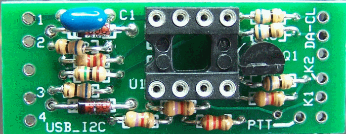
Bottom of the Board
Build Stage Testing
Resistance Tests
Test Setup
Perform this test with the ATTINY (U1) UNPLUGGED from SO1
- Measure resistances between the test points indicated in the table below
- Note: the resistance measurements should be within plus or minus 5% of the nominal value
In the next stage, we will connect the USB cable and apply power, via the USB port, to the board, with, and without U1 installed, measuring the voltages.
Test Measurements
| Testpoint | Units | Nominal Value | Author's | Yours |
|---|---|---|---|---|
| U1-3 to PTT | k ohm | 2.2 | 2.18 | _______ |
| U1-2 to CL | ohm | 68 | 67 | _______ |
| U1-6 to DA | ohm | 68 | 67 | _______ |
| USB-1 to K1 | k ohm | 4.7 | 4.6 | _______ |
| USB-1 to K2 | k ohm | 4.7 | 4.6 | _______ |
| USB-1 to U1-8 | ohm | 0 | 0 | _______ |
| USB-2 to U1-7 | ohm | 68 | 66.8 | _______ |
| USB-2 to USB-1 | k ohm | 2.268 | 2.27 | _______ |
| USB-3 to U1-5 | ohm | 68 | 66.8 | _______ |
| USB-3 to USB-1 | k ohm | 950 - 1,050 | 968 | _______ |
| USB-4 to U1-6 | M ohm | off the scale | off the scale | _______ |