External Connections Introduction
General
In this stage, we will:- Install the USB cable and test the interface under power (the +5 Vdc provided from the computer's USB port.
- Install the connector cable (and "plug") that will connect the interface to the RXTX V6.3 transceiver and/or the Lite + Xtall V8.3 RX, replacing their on-board ATTINY435 with the controls from the interface board.
- Optionally, install the PTT control lead that can connect to the PTT-I input of the RXTX V6.3 Transceiver. You only need this if you are going to control a transceiver.
- Optionally, install the connections for your keyer dot, dash, and common leads. Again, not needed if you are only going to control an RX (or do not intend to TX CW).
In the stage following this stage, we will actually hook the interface up to an interfacing rig (RX V8.3 or RXTX V6.3). The current stage focusses on all of the wires and cables needed to do that and on ensuring the AVR chip (ATTiny 85-20PU) is functioning OK
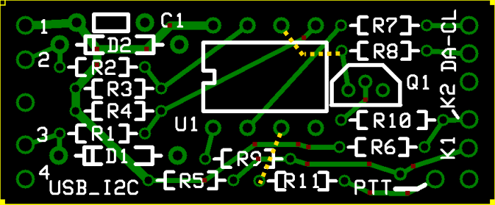
External Connections Schematic
(Resistor testpoints (hairpin, top, or left-hand lead), as physically installed on the board, are marked in the schematic with red dots)
(Click for Full Schematic)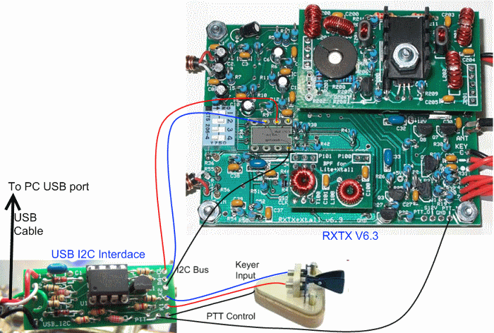
(above schematic has clickable areas that can be used for navigation)
External Connections Bill of Materials
Stage Bill of Materials
(resistor images and color codes courtesy of WIlfried, DL5SWB's R-Color Code program)
| Check | Designation | Component | Marking | Category | Orientation | Notes | Circuit |
|---|---|---|---|---|---|---|---|
| ❏ | cbl | USB 4 conductor 3' male | cable | External Connections | |||
| ❏ | control cable wire | misc hookup wire | misc | 3 short lengths of hookup wire (not provided with kit) | External Connections | ||
| ❏ | keyer wires (3) | misc hookup wire | misc | 3 short lengths of hookup wire (not provided with kit) | External Connections | ||
| ❏ | misc wire- PTT | misc hookup wire | misc | 1 short length of hookup wire (not provided with kit) | External Connections | ||
| ❏ | tubing | 3" Heat shrink tubing | misc | Once the kit is completed and fully tested, you can install the heatshrink tubing to protect the board. | External Connections | ||
| ❏ | SO2 | socket, machine, 8 pin |
 | socket | 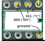 | External Connections | |
| ❏ | U1 | ATtiny 85-20 PU w/N15.12 Firmware | AVR ATTINY85-20PU
 | DIP 8 | Do not plug into sockect SO1 until first voltage test is completed. | External Connections |
External Connections Summary Build Notes
- Install USB Cable
- Install I2C control bus connector
- Install PTT control line (optional)
- Install keyer connection (optional)
- Apply heat shrink tubing (optional)
- Test the Stage
External Connections Detailed Build Notes
Top of the Board
Install USB Cable
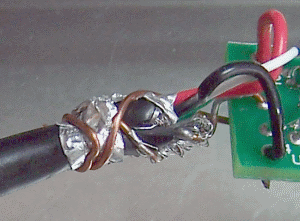
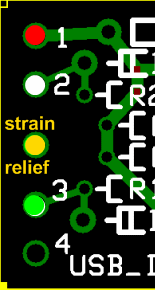
- Solder a short length of bus wire to the strain relief hole on the board (yellow hole, centered between holes 2 and 3 on the left-hand side of the board).
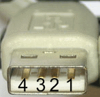
- Solder the 4 leads of the USB cable to the holes (1, 2, 3, and 4):
The leads should correspond in color
- 1=RED
- 2=WHITE
- 3=GREEN
- 4=BLACK
- as indicated in the associated photo (above).
- Wrap the strain relief wire firmly around the cable so as to let the bus wire take all the cable strain and protect the 4 USB leads from stresses/strains
- At this point, we can also plug in the ATTiny 85-20PU microprocessor chip that affects the control of the rig. The initial versions of this kit used the less capacious ATTiny 45-20PU and were programmed with an early version of the firmware. Current versions of the kit include (as of October 2009) the ATTiny 85-20PU chip with Fred PE0FKO's firmware version 15.12. That firmware can be configured to control all of the functionality of the RXTX V6.3 or the Automatic Bandpass Filter functionality of the Lite + Xtall RX V9.0. See Bob G8VOI's User Guide on configuring this chip and Fred PE0FKO's guide on obtaining running the configuration software.
| Check | Designation | Component | Marking | Category | Orientation | Notes |
|---|---|---|---|---|---|---|
| ❏ | cbl | USB 4 conductor 3' male | cable | |||
| ❏ | U1 | ATtiny 85-20 PU w/N15.12 Firmware | AVR ATTINY85-20PU
| DIP 8 | Take ESD precautions Do not plug into sockect SO1 until first voltage test is completed. |
Install I2C control bus connector
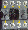
The I2C protocol for control of the Si570 requires two lines (in addition to a common ground line):
- The Clock line ("SCL") which provides clocking signals for Input Output data
- and the bidirectional serial data line ("SDA"), which carries output/input serial data across the interface.
Here, we will provide the connection over which the I2C control signals will move to the controlled rig (RX V8.3 or RXTX V6.3). You will have a choice of a NON-PERMANENT or a PERMANENT installation, as described below:
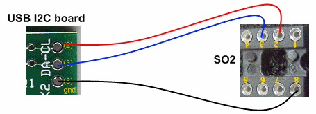
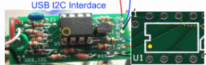
- A non-permanent connection, via soldering the cables into the top of the 8 pin machined socket provided in the kit for that purpose. In this latter case that socket, SO2, will act as a "plug" which can be plugged into the corresponding socket on the interfaced rig, as shown in the large interconnect image above that shows the USB_I2C mated to the RXTX V6.3.
- A permanent connection, to the RXTX, via direct soldering to holes provided on the RXTX board.
Non-Permanent Connection
- Select hookup wire whose diameter will fit into the small holes at the top of SO2
- Solder three 6" to 8" wires to the holes marked "DA" and "CL" and the unmarked (ground) hole below the "DA" hole in the upper right-hand corner of the board, as shown above. These correspond to the SDA data line ("DA") and the SCL clock line ("CL" signals which will control the Si570 on the V8.3 RX board or the V6.3 RXTX board.
The wire length should be chosen to fit your situation (but should be equal to the length used for the PTT control connection). - Solder the other ends of the three wires to the 8 pin socket SO2, which will serve as a "plug" to mate with the 12F683's socket on the interfaced rig. Note that this SO2 is provided in the USB I2C kit. Do NOT try to solder the three wires directly into the interfaced rig's 12F683 socket:
- Solder the SCL ("CL") wire to the TOP of SO2 at the hole for pin 2
- Solder the SDA ("DA") wire to the TOP of SO2 at the hole for pin 3
- Solder the ground wire to the TOP of SO2 at the hole for pin 8
- This will allow you to remove the 12F683 chip from its socket on the RX (U3) or RXTX (U6) board and replace it by plugging SO2, with its 3 leads, into the empty socket (carefully aligning the notched ends of the sockets).
Permanent Connection
- If you plan to use the interface permanently with your RXTX V6.3, you can dispense with SO2 and, instead, remove U6 (12F683) and SW1 from the RXTX board and solder the three leads to the corresponding holes (see photo below) in the SW1 footprint on the RXTX V6.3 board.
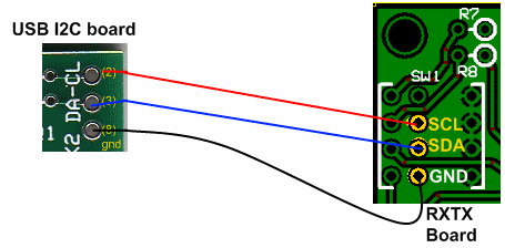
Showing the permanent connection to the three connect holes in the RXTX board (under SW1).
| Check | Designation | Component | Marking | Category | Orientation | Notes |
|---|---|---|---|---|---|---|
| ❏ | control cable wire | misc hookup wire | misc | 3 short lengths of hookup wire (not provided with kit) | ||
| ❏ | SO2 | socket, machine, 8 pin |
| socket | |
Install PTT control line (optional)
The SRv6.3 PTT_I was designed to be activated with +12V from the RS232C signal of the Rocky Interface, OR with +5V from other sources (e.g. a +5V uC signal, such as from the USB I2C board). Because you will have already connected the I2C bus's ground to the RXTX board, there is no need for an additional GND connection tor the PTT control, as the GND return may flow through the I2C bus.
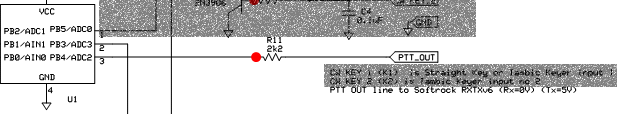
The USB I2C interface schematic shows that the
PTT_OUT (Rx = 0V, Tx = 5V) is to be connected to the SRv6.x. Although
not stated in the schematic, the connection is to SRv6.x's PTT_IN.
-

USB I2c Board
USB I2C Board - PTT Connection - Connect a 6" - 8" length of wire to the PTT hole at the bottom right of the USB I2C board. The wire length should be chosen to fit your situation (but should be equal to the length used for the I2C bus connection).
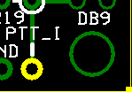
RXTX V6.3 Board- This will connect to the "PTT-I" hole on the RXTX board. You may want to use a connector arrangement in cases where you want the USB I2C Interface to be used on multiple Si570-driven RXTX and/or RX
| Check | Designation | Component | Marking | Category | Orientation | Notes |
|---|---|---|---|---|---|---|
| ❏ | misc wire- PTT | misc hookup wire | misc | 1 short length of hookup wire (not provided with kit) |
Install keyer connection (optional)

Connect three wires of appropriate length to the K1, K2, and ground leads and a suitable connector to the other end, such that your keyer inputs (and ground) can be fed to the USB I2C Interface board. The wire lengths should be chosen to suit your situation.
Note: The K1 input is for the DOT paddle and the K2 input is for the DASH paddle.
| Check | Designation | Component | Marking | Category | Orientation | Notes |
|---|---|---|---|---|---|---|
| ❏ | keyer wires (3) | misc hookup wire | misc | 3 short lengths of hookup wire (not provided with kit) |
Apply heat shrink tubing (optional)
Tony supplies a piece of heat shrink tubing to allow you to encapsulate the completed board in a protective shield
| Check | Designation | Component | Marking | Category | Orientation | Notes |
|---|---|---|---|---|---|---|
| ❏ | tubing | 3" Heat shrink tubing | misc | Once the kit is completed and fully tested, you can install the heatshrink tubing to protect the board. |
External Connections Completed Stage
Top of the Board

External Connections Testing
Voltage Tests - U1 Not Installed
Test Setup
Note: this and the following tests are performed with no connections being made yet to the interfacing rig(s).
This test measures the voltages of a powered up board with the ATTINY (U1) NOT connected.
- Connect the USB plug to a USB port on your computer.
- Measure the voltages at the testpoints specified in the table below. All voltages are WRT ground
Test Measurements
| Testpoint | Units | Nominal Value | Author's | Yours |
|---|---|---|---|---|
| PTT | mVdc | 0 - 100 | 3.6 | _______ |
| K1 | Vdc | 5 | 5.03 | _______ |
| K2 | Vdc | 5 | 5.03 | _______ |
| SO1 Pin 1 | Vdc | 5 | 5.03 | _______ |
| SO1 Pin 4 | Vdc | 0 | 0 | _______ |
| SO1 Pin 5 | mVdc | 60 - 100 | 98.9 | _______ |
| SO1 Pin 6 | Vdc | varying (clocking activity) | observed | _______ |
| SO1 Pin 7 | Vdc | 2.5-3.5 | 3.02 | _______ |
| SO1 Pin 8 | Vdc | 5 | 5.03 | _______ |
Voltage Tests - U1 Installed
Test Setup
Once we are satisfied with the voltages from the previous tests, we measure the voltages with U1 installed.
- Unplug the USB cable
- Taking ESD precautions, plug the ATTINY (U1) chip into socket SO1. Note carefully the orientation. The dimple/dot on U1 signifies the location of pin 1 and, when installed, should be to the left.
- Apply power by plugging the USB plug into a USB port on your computer
- Measure the voltages WRT ground at the testpoints indicated in the table below
Jan G0BBL adds: "Please note where i put down "varying" it generally means floating pins because the cable to V8.3 pcb is not plugged in. IF you have a meter with low impedence then floating inputs tend to drift towards 0 volt."
Test Measurements
| Testpoint | Units | Nominal Value | Author's | Yours |
|---|---|---|---|---|
| USB cable +5 Vdc lead | Vdc | 5 | 4.98 | _______ |
| SO1 Pin 1 | Vdc | 5 | 4.98 | _______ |
| SO1 Pin 2 | Vdc | varying | varying | _______ |
| SO1 Pin 3 | Vdc | 0 | 0 | _______ |
| SO1 Pin 4 | Vdc | 0 | 0 | _______ |
| SO1 Pin 5 | mVdc | 90 - 110 | 100 | _______ |
| SO1 Pin 6 | Vdc | varying | varying | _______ |
| SO1 Pin 7 | Vdc | 2.5 | 2.49 | _______ |
| SO1 Pin 8 | Vdc | 5 | 4.98 | _______ |
USB View test
Test Setup
This test is one that is recommended in Tom Baier's DG8SAQ AVR Troubleshooting Guide. You will need to download the microsoft USB View program, made available on Tom's website. Once you downlod the zip file you can open it up and execute the program from inside the zip file.
Setup:
- If you have not already done so, plug in the AVR chip, paying close attention to the orientation - see above photo
- Plug your USB cable into a USB port on the PC
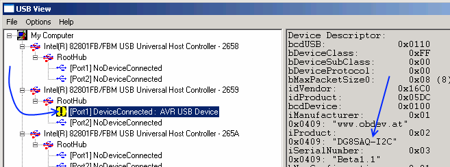
- You should see results similar to the above
- If, after plugging in your USB device, you see, instead, a message saying that the device is unrecognized, then you need to follow the troubleshooting hints in Tom's document, found in the Yahoo Group's Files section in the DG8SAQ folder. A copy of that guide is provided for your convenience here.
Functional Test of USB Control
Test Setup
AVR Chip Configuration
Install the USB driver software on your PC
If you have not already done so, install the latest USB driver on your PC. This driver is found at Fred Krom's PE0FKO website in a USB driver zip file. The file is located quite a ways down in the web page (hint: do a "Find" on "Installing the PC driver software" to get to the link to the latest PC Driver zip file).
Download the zip file and extract the it to a temporary directory (on the Desktop). Then, plug in the device and it will show "Found new hardware DG8SAQ-I2C". Direct Windows' driver installation wizard to the directory where the software was temporarily stored and finish installing the driver.
Configure the AVR Chip
This step involves downloading an executable program and an associated DLL and running the program to configure the AVR chip to your desired settings.
- Download the following from
Fred's CFGSR web page into the directory of your choice
(hint: do a "Find" on "Download"):
- Fred PE0FKO's Configuration Tool Program: CFGR.EXE
- Softrock DLL(to handle the protocol and the USB interface): SRDLL.dll
- Run the CFGR.exe program and follow the instructions on Fred's site.
Functional Test Setup
The functional testing of this kit assumes you will be using the Rocky SDR program to control your Local Oscillator and set your center frequencies.
The following steps outline how to set up Rocky for this (and later) tests:
- Download Rocky V3.6 and install it
- Run Rocky and enable the Si570 support in Rocky by ticking the "Use Si570-USB" check box in the Settings/DSP dialog. Do not change the "address" and "divider" settings.
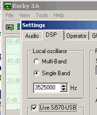
- In the In the "Hz" fiield, type in
7046000to set Rocy's default center frequency to 7.046 MHz. - Set up Rocky for RX=only:
- Click on
View/Settings and the"Audio"tab -
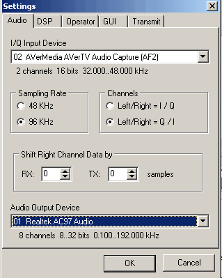
- Select the
"I/Q Input Device"to be the your on-board sound card - Select the
"Audio Output Device"to be your on-board sound card - Click on the
"Transmit"tab -
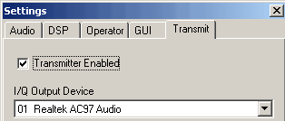
- Clear the
"Transmitter Enable"checkbox to disable transmit mode
- Click on
The PC is now set up to use Rocky to control the Si570 Local Oscillator.