Introduction
This is the home page for the Detailed Builder's Notes for the Softrock "Lite + USB Xtall" V9.0 Software Defined Radio receiver, the latest in a series of SDR kits offered by Tony Parks KB9YIG.
The intent in providing these detailed instructions is to help the less experienced builder through what might otherwise be a daunting task. The instructions provide a stage-by-stage build process, allowing the builder to build a single stage and then test it ("sanity check") before moving on to the next stage.
Much of the documentation was initially developed entirely from the schematic and from the earlier V8.3/8.4 documentation. Over time, the author may post changes to the affected web pages, as necessary. You should check periodically to see if there have been any revisions, especially in the area of Stage-end tests. If your browser is caching pages, you may need to hit the "refresh" key (F5 on IE and Firefox) to get the latest version of the page.
These notes can be downloaded as a PDF file here. Thanks to Craig AB9IV.
Ordering Information
Prices and availability of the kit and its options are found at the Softrock Ordering Website.
Build Stages and Schematic
Construction Stages and Theory of Operation
(Click on a stage to view its detailed builders' notes)
Each stage will have a subset of the overall schematic diagram. Each sub-schematic is annotaded with clickable text to show "from/to" stages. The user can click on the text and link to the appropriate stage.
The schematics are annotated with red dots to designate the resistors' hairpin leads (or for a flat-mounted resistor, the left-hand or top lead).
To view the schematic diagram for the entire receiver, see Overall Schematic Diagram from Tony's original documentation.
For the more experienced builder, each stage has a "Summary Build Steps" section which outlines the sequencing of tasks within the stage and provides a link to the testing stage (bypassing the detailed installation notes).
For the most experienced builder, see the "Terse" builder's notes below.
For the rest os us, detail construction steps and tests are provided in each stage and will be highlighted by special Icons:
A step in the detailed build section
A test operation in the Testing section
A test operation requiring an HF transceiver.
An optional test using an oscilloscope.
Any comments or corrections should be directed to the author, Robby WB5RVZ, and would be most appreciated.
Theory of Operation
This kit incorporates the new SI570 programmable oscillator, along with a USB-coupled microcontroller that allows an SDR program on the PC to tune that oscillator to any desired"center" frequencies with which to drive the basic Softrock receiver.
The kit covers both types of SI570 oscillators: the CMOS version and the LVDS version. The only differences are with respect to two components, R25 and U8 (see the Bill of Materials) .
The receiver builds on the earlier Softrock RX-Lite receiver. The problem with that earlier receiver was - as "Softrock" implies - it was pretty much rockbound. For a given crystal value, you could receive one or two "bands", centered on a frequency that was one-fourth the crystal frequency. Depending upon the sound card used, the bandwidth of the receiver would be +/- 24 kHz around the center frequency or +/- 48 kHz around the center frequency, depending upon the sound card's sampling bandwidth.
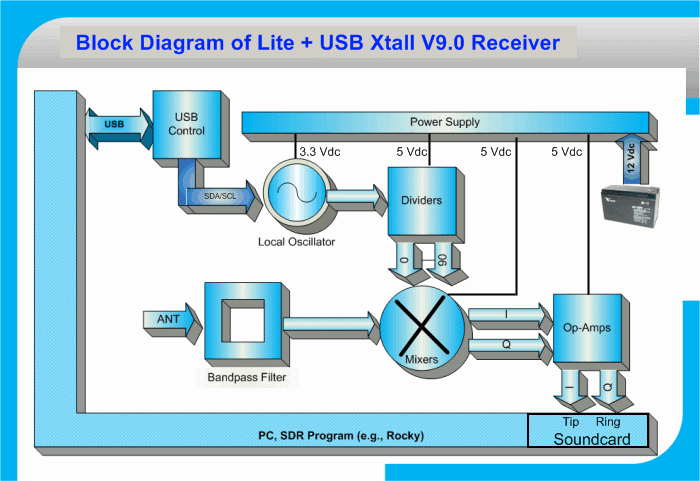
In the block diagram above (which is almost identical to the block diagram for a simple direct conversion receiver), the Bandpass Filter, Mixer, and OpAmps stages are essentially the same as those on the RX-Lite. The Local Oscillator and Dividers stages replace the crystal-based LO and divider chain of the original. However, the essence remains:
- the local oscillator develops a signal that is a 4X multiple of the center frequency and the dividers bring the signal to the desired center frequency and into quadrature (90° phase difference between the two outputs of the chain).
- These 2 signals are fed to the Mixer stage, which down-converts the "chunk" of RF that is in the passband of the bandpass filters into 2 "chunks" of audio representing the difference between the incoming RF and the LO quadrature signals.
- These 2 AF signals are identical, and 90° out of phase with each other. They are amplified in the Op-Amps stage and fed into the PC's sound card to be digitized and processed.
- An essential part of that digital signal processing is using the quadrature streams to tease out the signals that are above the center frequency from those that are below the center ferequency, yielding a spectrum centered on the center frequency.
The real advance here is the use of a programmable oscillator (SI570) in the local oscillator circuit and a USB control circuit to program the Si570. (The USB control circuit also provides PTT switching outputs and keyer/stgraight key inputs for the SDR software running on the PC, but these are not needed for RX only operation). This setup allows the user to select any desired center frequency. This is a major advance over the Version 8.3 receiver, which only permitted switch selection of up to 16 pre-programmed center frequencies and leaves the rockbound RX Lite in the dust!
The other advance is changing the design of the bandpass filters to allow for removable filter boards (this radio uses the same BPFs as the Version 8.3 BPFs). Together these design changes add a multiband capability to the Softrock platform and open it up to follow-on designs that will provide even greater frequency agility.
See, also, the Detailed Theory of Operation discussion.
Bill of Materials
Each stage of construction will be preceded by a detailed bill of the materials for that stage, ordered in the sequence in which the different components are to be installed.
For reference and inventorying purposes, the overall bill of materials is provided in a separate "Bill of Materials" page.
Terse Build Notes for the "Experts"
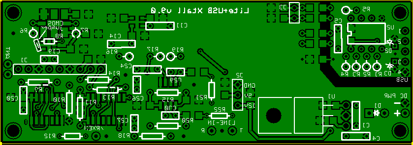
Tony's original build instructions for the expedited, "non-staged" approach are provided here for reference. If you plan to follow the staged construction approach outlined in this and subsequent pages, do not attempt to follow the steps listed below.Board Topside
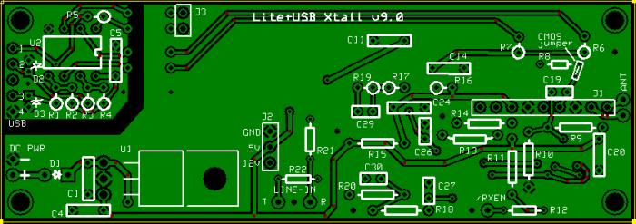
Board Bottomside
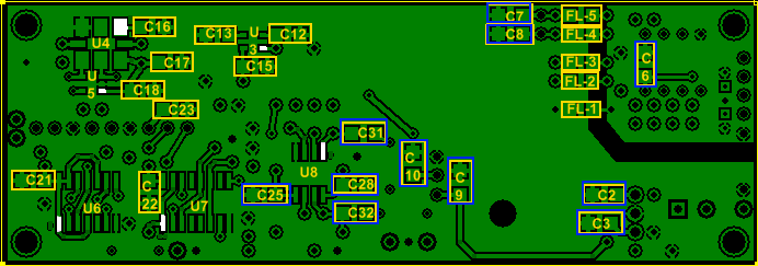
Board Bottomside (with reversed topside silkscreen overlaid)
Do not follow the summary approach below unless you are an accomplished builder and feel no need to build the kit using the staged approach.
Tasks for "Stuff-the-Board-and-Then-Test" approach (said Tom tersely)
- Install all SMT Capacitors to bottom of board (see graphic, above) , except for those around U3 (C12, C13m abd C15) and (if U5 is used) C18.
- Install Five pin SMT 3.3V Voltage Regulator, U3, to bottom of board.
Make sure U3 leads are well-centered on their pads, then tack the IC in place by careful soldering of one lead. Apply heat to pin to reposition U3 and, when properly positioned, carefully solder the other leads.
Use solder wick to remove excess solder or solder bridges between pins. - If using LVDS version of Si570, install U5, Fin1002, on bottom of board in same careful fashion as U3. U5 is NOT installed if the Si570 is the CMOS version.
- Install remaining SMT capacitors (C12, C13, and C15)
- Install U4, Si570, on bottom of board with careful soldering as with U3. Note that there are 8 "pins" to be soldered.
- Install remaining SOIC SMT ICs to bottom of board (if an IC in the kit fits a location, it is the correct IC for that location).
- Mount 5V Voltage regulator U1, LM7805, to top of board with a 4-40 machine screw, #4 start lockwasher, and hex nut, attaching the tab of U1 to the board.
- Mount the 2 and 3 pin sockets, J3 and J2, in the J3 and J2 locations.
- Mount 9-pin socket J1 in its location.
- Install resistors R1-R22 on top of the board, with R1-R7, R16-R17, and R19mounted
"hairpin" style.
All other resistors are mounted flat.
Note: R8 is NOT installed if the Si570 is the CMOS version - Install capacitors to the top of the board in the locations shown on the silkscreen.
- Install the socket for U3 on top of board.
- Diodes D1-D3 on top of board in hairpin fashion with diode body above each round pad.
- Connect a shorting wire in the CMOS jumper location if the Si570 is the CMOS version.
- Connect a shorting wire between the /RXEN hole and the ground hole immediately to its left.
- Build desired band pass filter board(s) and mount on J1 such that the 3 header pins go to J1's left-most 3 pin sockets.
Detailed Build Notes
If you prefer to take the more methodical, "build a little, test a little, ...." staged approach to building this kit, this web site is for you. In the pages that follow this home page, you will find the notes for the construction and testing of each of the stages of the build.
The build will go through the following stages
- Receipt and Inventory of the Kit using the Bill of Materials
- Build and test the Power Supplies (5Vdc and 3.3 Vdc)
- Build and test the USB Control Circuit
- Build and test the Local Oscillator
- Build and test the Divider STage
- Build and test the Operational Amplifier Stage
- Build and test the Mixer Stage
- Build and test the Bandpass Filter Board(s)
- Connect the completed board to the outside world.
Each stage will Have the same basic sections:
- Introduction and theory of operation
- Schematic - a subset of the overall schematic diagram
- Bill of Materials - a build sequence ordered set of the items to be installed in the stage
- Summary Build Instructions - a summary of the steps in the stage
- Detailed Build Instructions - the step-by-step, detailed tasks of the build
- Testing - one or more tests that can be conducted to validate the built stage
Testing
Most of the tests specified in these pages can be accomplished with a moderately priced digital multimeter. Some tests using more sophisticated tools may be specified, but are not really essential to successfully building and testing this radio.
Measurements specified in the tests must be considered approximate and the tester should expect a fairly wide (+/- 1--20%) range of values around the specified values.
Tests will be identified by the following icons:
- A test that requires no more than your DMM
- An optional test that may require HF transceiver to transmit into a dummy or receive through a loosely coupled antenna wire one or more test frequencies
- An optional test which requires an oscilloscope
Background Info
Tools
Soldering
View above video example on Youtube
- Read the Primer on SMT Soldering at the Sparkfun site. It is a very good read and it speaks great truths. Then take the time to watch the video tutorial on soldering an SOIC SMD IC.
- For more general "how-tos" on soldering, Craig KB5UEJ highly recommends the videos at this site.
- "Splashover": Be careful when soldering SMT components to the bottom of the board. In some cases There are holes through which topside component leads must pass and which can easily get clogged with "solder splashover", where the hole is very close to an SMT pad.
- Solder Stations. Don't skimp here. Soldering deficiencies account for 80 percent of the
problems uncovered in troubleshooting. It is preferable to have an ESD-safe station, with a
grounded tip. A couple of good stations that are relatively inexpensive are:
-
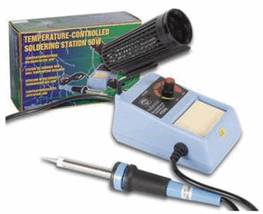 Velleman VTSS5U 50W Solder Station (approx $20 at Frys)
 -
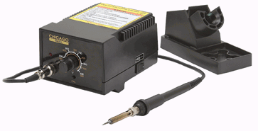 Harbor Freight ESD Solder Station (under $50)
-
Electro Static Discharge (ESD) Protection
- Whenever you see the symbol on the left, this means to take ESD precautions:
- Avoid carpets in cool, dry areas.
- Leave PC cards and memory modules in their anti-static packaging until ready to be installed.
- Dissipate static electricity before handling any system components (PC cards, memory modules) by touching a grounded metal object, such as the system unit unpainted metal chassis.
- If possible, use antistatic devices, such as wrist straps and antistatic mats (see Radio Shack's Set for $25 or the JameCo AntiStatic mat for $15)).
- Always hold a PC card or memory module by its edges. Avoid touching the contacts and components on the component.
- Before removing chips from their insulator, put on the wrist strap connected to the ESD mat. All work with CMOS chips should be done with the wrist strap on.
- As an added precaution before first touching a chip, you should touch a finger to a grounded metal surface.
- If using a DMM, its outside should be in contact with the ground of the ESD mat, and both leads shorted to this ground before use.
- See the review of ESD Precautions at this link.
Work Area
- You will need a well-lit work area and a minimum of 3X magnification (the author uses a cheap magnifying flourescent light with a 3X lens. This is suplemented by a hand-held 10 X loupe - with light - for close-in inspection of solder joints and SMT installation.
- You should use a cookie sheet or baking pan (with four sides raised approximately a half an inch) for your actual work space. It is highly recommended for building on top of in order to catch stray parts, especially the tiny SMT chips which, once they are launched by an errant tweezer squeeze, are nigh on impossible to find if they are not caught on the cookie sheet.
Misc Tools
- It is most important to solidly clamp the PCB in a holder when soldering. A "third-hand" (e.g., Panavise or the Hendricks kits PCB Vise) can hold your board while soldering. In a pinch, you can get by with a simple third-hand, alligator clip vise. Jan G0BBL suggests "A very cheap way is to screw a Large Document Clip to a woodblock which will clamp the the side of a PCB."
- Magnifying Head Strap
- Tweezers (bent tip is preferable).
- Diagonal side cutters.
- Small, rounded jaw needle-nose pliers.
- Set of jewelers' screwdrivers
- An Exacto knife.
- Fine-grit emery paper.