Introduction
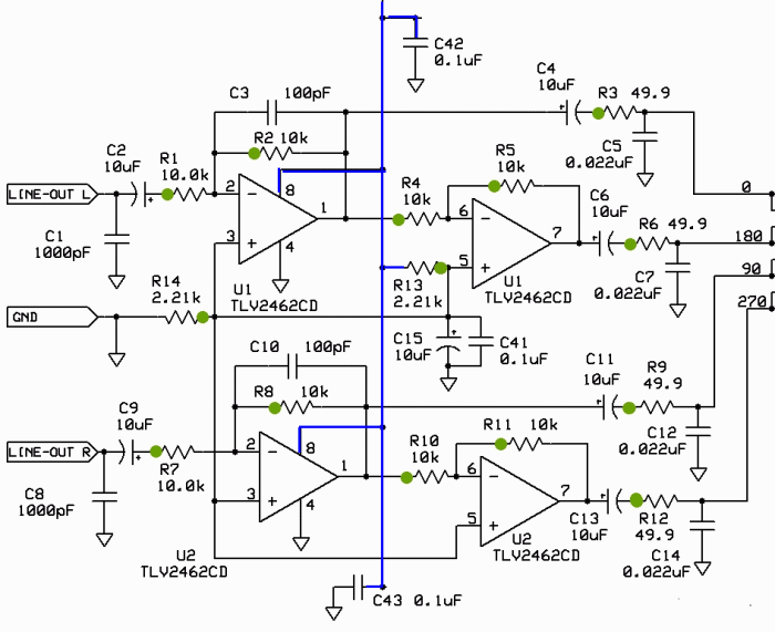
This stage has a pretty large part count.. It consists of four unitary gain op-amps, arranged in pairs, one per stereo line out signal into the board. The left channel's input resolves to two signals: 0° and 180°. The right channel's input resolves to two signals: 90° and 270°.
These four outputs will be muxed together in the mixer stage to produce the desired exciter output (thus, the term Quadrature Sampling Exciter (QSE)).
Schematic
(Click for full TX Schematic)
Summary Build Notes
- Install Ceramic Caps C1, C3, C5, C7, C8, C10, C12, and C14
- Install Electrolytic Caps C2, C4, C6, C9, C11, C13, and C15
- Install Resistors R1-R14
- Install U1 and U2
- Test the Stage
Bill of Materials
| Check | Designation | Component | (Color) Code | Type | Qty | Notes |
|---|---|---|---|---|---|---|
| [__] | C01 | 1000 pF | 102 | ceramic | 1 | |
| [__] | C02 | 10 uF 16V | electrolytic | 1 | E=+ | |
| [__] | C03 | 100pF | 101 | ceramic | 1 | |
| [__] | C04 | 10 uF 16V | electrolytic | 1 | S=+ | |
| [__] | C05 | 0.022 uF | 223 | ceramic | 1 | |
| [__] | C06 | 10 uF 16V | electrolytic | 1 | N=+ | |
| [__] | C07 | 0.022 uF | 223 | ceramic | 1 | |
| [__] | C08 | 1000 pF | 102 | ceramic | 1 | |
| [__] | C09 | 10 uF 16V | electrolytic | 1 | E=+ | |
| [__] | C10 | 100pF | 101 | ceramic | 1 | |
| [__] | C11 | 10 uF 16V | electrolytic | 1 | W=+ | |
| [__] | C12 | 0.022 uF | 223 | ceramic | 1 | |
| [__] | C13 | 10 uF 16V | electrolytic | 1 | N=+ | |
| [__] | C14 | 0.022 uF | 223 | ceramic | 1 | |
| [__] | C15 | 10 uF 16V | electrolytic | 1 | E=+ | |
| [__] | R01 | 10 k | brown-black-black-red-brown | Resistor 1% | 1 | N-S |
| [__] | R02 | 10 k | brown-black-black-red-brown | Resistor 1% | 1 | E-W |
| [__] | R03 | 49.9 | yellow-white-white-gold-brown | Resistor 1% | 1 | S-N |
| [__] | R04 | 10 k | brown-black-black-red-brown | Resistor 1% | 1 | N-S |
| [__] | R05 | 10 k | brown-black-black-red-brown | Resistor 1% | 1 | S-N |
| [__] | R06 | 49.9 | yellow-white-white-gold-brown | Resistor 1% | 1 | E-W |
| [__] | R07 | 10 k | brown-black-black-red-brown | Resistor 1% | 1 | S-N |
| [__] | R08 | 10 k | brown-black-black-red-brown | Resistor 1% | 1 | E-W |
| [__] | R09 | 49.9 | yellow-white-white-gold-brown | Resistor 1% | 1 | E-W |
| [__] | R10 | 10 k | brown-black-black-red-brown | Resistor 1% | 1 | N-S |
| [__] | R11 | 10 k | brown-black-black-red-brown | Resistor 1% | 1 | S-N |
| [__] | R12 | 49.9 | yellow-white-white-gold-brown | Resistor 1% | 1 | S-N |
| [__] | R13 | 2.21 k | red-red-brown-brown-brown | Resistor 1% | 1 | S-N |
| [__] | R14 | 2.21 k | red-red-brown-brown-brown | Resistor 1% | 1 | W-E |
| [__] | U1 | TLV2462 | IC SOIC-8 dual Op-Amp | 1 | (bottom) | |
| [__] | U2 | TLV2462 | IC SOIC-8 dual Op-Amp | 1 | (bottom) |
Detailed Build Notes
- Need to do topside components first, as many holes for these are very close to the IC pads on the bottomside - avoiding solder splashover
Install the 8 Ceramic Capacitors
| Check | Designation | Component | (Color) Code | Type | Qty | Notes |
|---|---|---|---|---|---|---|
| [__] | C01 | 1000 pF | 102 | ceramic | 1 | |
| [__] | C03 | 100pF | 101 | ceramic | 1 | |
| [__] | C05 | 0.022 uF | 223 | ceramic | 1 | |
| [__] | C07 | 0.022 uF | 223 | ceramic | 1 | |
| [__] | C08 | 1000 pF | 102 | ceramic | 1 | |
| [__] | C10 | 100pF | 101 | ceramic | 1 | |
| [__] | C12 | 0.022 uF | 223 | ceramic | 1 | |
| [__] | C14 | 0.022 uF | 223 | ceramic | 1 |
Install the 7 Electrolytic Capacitors
Note the orientation of the positive lead ("notes" column, below)
| Check | Designation | Component | (Color) Code | Type | Qty | Notes |
|---|---|---|---|---|---|---|
| [__] | C02 | 10 uF 16V | electrolytic | 1 | E=+ | |
| [__] | C04 | 10 uF 16V | electrolytic | 1 | S=+ | |
| [__] | C06 | 10 uF 16V | electrolytic | 1 | N=+ | |
| [__] | C09 | 10 uF 16V | electrolytic | 1 | E=+ | |
| [__] | C11 | 10 uF 16V | electrolytic | 1 | W=+ | |
| [__] | C13 | 10 uF 16V | electrolytic | 1 | N=+ | |
| [__] | C15 | 10 uF 16V | electrolytic | 1 | E=+ |
Install the 14 Resistors
Note: orientation is in "Notes" column below.
| Check | Designation | Component | (Color) Code | Type | Qty | Notes |
|---|---|---|---|---|---|---|
| [__] | R01 | 10 k | brown-black-black-red-brown | Resistor 1% | 1 | N-S |
| [__] | R02 | 10 k | brown-black-black-red-brown | Resistor 1% | 1 | E-W |
| [__] | R03 | 49.9 | yellow-white-white-gold-brown | Resistor 1% | 1 | S-N |
| [__] | R04 | 10 k | brown-black-black-red-brown | Resistor 1% | 1 | N-S |
| [__] | R05 | 10 k | brown-black-black-red-brown | Resistor 1% | 1 | S-N |
| [__] | R06 | 49.9 | yellow-white-white-gold-brown | Resistor 1% | 1 | E-W |
| [__] | R07 | 10 k | brown-black-black-red-brown | Resistor 1% | 1 | S-N |
| [__] | R08 | 10 k | brown-black-black-red-brown | Resistor 1% | 1 | E-W |
| [__] | R09 | 49.9 | yellow-white-white-gold-brown | Resistor 1% | 1 | E-W |
| [__] | R10 | 10 k | brown-black-black-red-brown | Resistor 1% | 1 | N-S |
| [__] | R11 | 10 k | brown-black-black-red-brown | Resistor 1% | 1 | S-N |
| [__] | R12 | 49.9 | yellow-white-white-gold-brown | Resistor 1% | 1 | S-N |
| [__] | R13 | 2.21 k | red-red-brown-brown-brown | Resistor 1% | 1 | S-N |
| [__] | R14 | 2.21 k | red-red-brown-brown-brown | Resistor 1% | 1 | W-E |
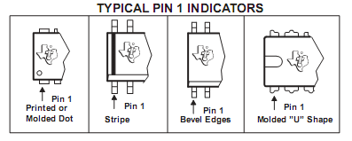
Install the 2 SMT Op-Amps
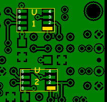
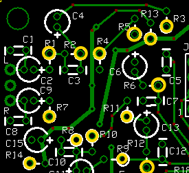
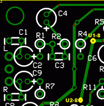
Note: one of the pin indicators (below) refers to a molded "U" on the chip. Do not confuse this with the
"U1" and "U2" annotations in the above picture of the IC placement on the underside of the board.
Thanks to Ross OK5AZ for catching this.
Install U1, U2,
Watch out for solder splashover on any adjacent, open holes
| Check | Designation | Component | (Color) Code | Type | Qty | Notes |
|---|---|---|---|---|---|---|
| [__] | U1 | TLV2462 | IC SOIC-8 dual Op-Amp | 1 | (bottom) | |
| [__] | U2 | TLV2462 | IC SOIC-8 dual Op-Amp | 1 | (bottom) |
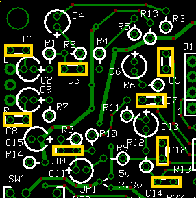
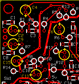
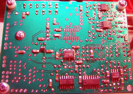
Completed Board
Topside
Bottomside
Testing
Current Limited Power Test
- Connect a 100 ohm resistor in series with the power line and apply 12 V dc power
- the current should be less than 120 mA (nominally 100 mA)
- Measure the voltage WRT ground at the +5 V and at the 3.3 Vdc testpoints.
- A voltage of around 2 V dc indicates the power rails are not shorted
- Remove the current-limiting resistor. Subsequent tests in this stage are with the current-limiting resistor OUT of the circuit.
Current Draw
- Without Limiting resistor the draw should be < 102 mA
- Your measurement: ________________________________
Op-Amp Voltage Divider (R13/R14)
- R13/R14 form a voltage divider to halve the 5 Vdc rail
- measure the voltage WRT ground at the R14 hairpin.
- You should see nominaly 2.5 Vdc (actual would range between 2.4 and 2.5 Vdc)
- Your Measurement: _________________________________
Op-Amp Pin Voltages
- If the voltage divider tests out OK, measure the voltages at the pins of U1 and U2 using the table below
- You should measure at the actual pins on the ICs as well as using the convenient resistor hairpin testpoints
Actual values in the 2.5 nominal measurements will range from 2.4 to 2.5 Vdc
| Pin | Nominal Value | Author Result | Your Measurement |
|---|---|---|---|
| 1 (R4 hairpin) | ½ 5V rail | 2.48 | |
| 2 (R2 hairpin) | ½ 5V rail | 2.48 | |
| 3 (R14 hairpin) | ½ 5V rail | 2.48 | |
| 4 | 0 (gnd) | 0 | |
| 5 (R13 hairpin) | ½ 5V rail | 2.48 | |
| 6 (R5 hairpin) | ½ 5V rail | 2.48 | |
| 7 | ~2.5 Vdc | ½ 5V rail | |
| 8 See testpoint picture above | 5V rail | 4.96 |
| Pin | Nominal Value | Author Result | As Measured |
|---|---|---|---|
| 1 (R10 hairpin) | ½ 5V rail | 2.48 | |
| 2 (R8 hairpin) | ½ 5V rail | 2.48 | |
| 3 (R14 hairpin) | ½ 5V rail | 2.48 | |
| 4 | 0 (gnd) | 0 | |
| 5 (R13 hairpin) | ½ 5V rail | 2.48 | |
| 6 (R11 hairpin) | ½ 5V rail | 2.48 | |
| 7 | ½ 5V rail | 2.48 | |
| 8 See testpoint picture above | 5V rail | 4.96 |
Op-Amp Function
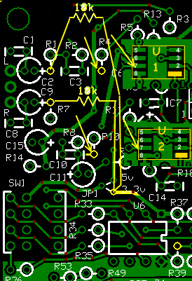
- Connect a test lead with a spare 10 kOhm resistor in series between R1 hairpin and the 3.3 V test point at JP1 (alternatively you can clip to the R39 or R40 hairpin for a 3.3V source)
- Power up the board
- Measure the voltage at R4 hairpin. It should be ½ the 5 V rail - 0.4 Vdc (about 2.1 Vdc)
- Measure the voltage at pin 7 of U1. It should be ½ the 5 V rail + 0.4 Vdc (about 2.9 Vdc)
- Disconnect the lead and resistor from R1 and connect it to bridge between R7 hairpin and the 3.3 V test point (JP1, R39, or R40)
- Measure the voltage at R10 hairpin. It should be ½ the 5 V rail - 0.4 Vdc (about 2.1 Vdc)
- Measure the voltage at pin 7 of U2. It should be ½ the 5 V rail + 0.4 Vdc (about 2.9 Vdc)
| Test Point | Nominal | Your Measurement |
|---|---|---|
| R4 hairpin - R1 bridged | around 2.1 Vdc | |
| U1, Pin 7 - R1 bridged | around 2.9 Vdc | |
| R4 hairpin - R1 unbridged | ½ 5V rail | |
| U1, Pin 7 - R1 unbridged | ½ 5V rail | |
| R10 hairpin - R7 bridged | around 2.1 Vdc | |
| U2, Pin 7 - R7 bridged | around 2.9 Vdc | |
| R10 hairpin - R7 unbridged | ½ 5V rail | |
| U2, Pin 7 - R7 unbridged | ½ 5V rail |