Introduction
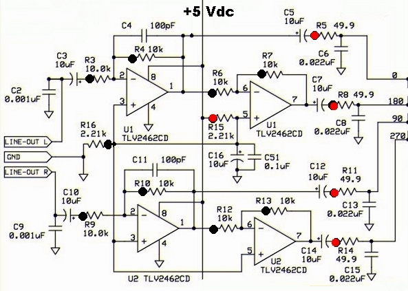
This stage has a pretty large part count. It consists of four unitary gain op-amps, arranged in pairs, one per stereo line out signal into the board. The left channel's input resolves to two signals: 0° and 180°. The right channel's input resolves to two signals: 90° and 270°.
These four outputs will be muxed together in the mixer stage to produce the desired exciter output (thus, the term Quadrature Sampling Exciter (QSE)).
Schematic
Bill of Materials
| Designation | Value | Orientation |
|---|---|---|
| C02 | 0.001uF, ceramic, 10% | n/a |
| C03 | 10uF/16 VDC Electrolytic | East-West |
| C04 | 100pF, ceramic, 5% | n/a |
| C05 | 10uF/16 VDC Electrolytic | West-East |
| C06 | 0.022uF, ceramic, 5% | n/a |
| C07 | 10uF/16 VDC Electrolytic | North-South |
| C08 | 0.022uF, ceramic, 5% | n/a |
| C09 | 0.001uF, ceramic, 10% | n/a |
| C10 | 10uF/16 VDC Electrolytic | East-West |
| C11 | 100pF, ceramic, 5% | n/a |
| C12 | 10uF/16 VDC Electrolytic | West-East |
| C13 | 0.022uF, ceramic, 5% | n/a |
| C14 | 10uF/16 VDC Electrolytic | West-East |
| C15 | 0.022uF, ceramic, 5% | n/a |
| C16 | 10uF/16 VDC Electrolytic | South-North |
| R03 | 10.0 K, 1/4 W, 1% | East-West |
| R04 | 10.0 K, 1/4 W, 1% | East-West |
| R05 | 49.9, 1/4W, 1% | East-West |
| R06 | 10.0 K, 1/4 W, 1% | East-West |
| R07 | 10.0 K, 1/4 W, 1% | South-North |
| R08 | 49.9, 1/4W, 1% | East-West |
| R09 | 10.0 K, 1/4 W, 1% | South-North |
| R10 | 10.0 K, 1/4 W, 1% | East-West |
| R11 | 49.9, 1/4W, 1% | East-West |
| R12 | 10.0 K, 1/4 W, 1% | East-West |
| R13 | 10.0 K, 1/4 W, 1% | South-North |
| R14 | 49.9, 1/4W, 1% | North-South |
| R15 | 2.21 K, 1/4W, 1% | North-South |
| R16 | 2.21 K, 1/4W, 1% | South-North |
| C51 | 0.1uF, smt 1206 | smt |
| C52 | 0.1uF, smt 1206 | smt |
| U01 | TLV2462CD op-amp, SOIC 8 | SOIC 8 |
| U02 | TLV2462CD op-amp, SOIC 8 | SOIC 8 |
Build Notes
- Need to do topside components first, as many holes for these are very close to the IC pads on the bottomside - avoiding solder splashover
Install the 8 Ceramic Capacitors
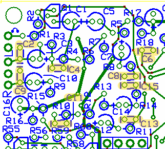
Install C2, C4, C6, C8, C9, C11, C13, and C15
| Designation | Value | Orientation |
|---|---|---|
| C02 | 0.001uF, ceramic, 10% | n/a |
| C04 | 100pF, ceramic, 5% | n/a |
| C06 | 0.022uF, ceramic, 5% | n/a |
| C08 | 0.022uF, ceramic, 5% | n/a |
| C09 | 0.001uF, ceramic, 10% | n/a |
| C11 | 100pF, ceramic, 5% | n/a |
| C13 | 0.022uF, ceramic, 5% | n/a |
| C15 | 0.022uF, ceramic, 5% | n/a |
Install the 7 Electrolytic Capacitors
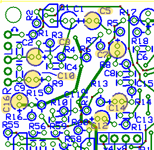
Install C3, C5, C7, C10, C12, C14, and C16
| Designation | Value | Orientation |
|---|---|---|
| C03 | 10uF/16 VDC Electrolytic | East-West |
| C05 | 10uF/16 VDC Electrolytic | West-East |
| C07 | 10uF/16 VDC Electrolytic | North-South |
| C10 | 10uF/16 VDC Electrolytic | East-West |
| C12 | 10uF/16 VDC Electrolytic | West-East |
| C14 | 10uF/16 VDC Electrolytic | West-East |
| C16 | 10uF/16 VDC Electrolytic | South-North |
Install the 14 Resistors
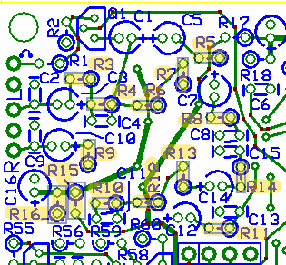
Install Resistors R3, R4, R5, R6, R7, R8, R9, R10, R11, R12, R13, R14, R15, R16
| Designation | Value | Orientation |
|---|---|---|
| R03 | 10.0 K, 1/4 W, 1% | East-West |
| R04 | 10.0 K, 1/4 W, 1% | East-West |
| R05 | 49.9, 1/4W, 1% | East-West |
| R06 | 10.0 K, 1/4 W, 1% | East-West |
| R07 | 10.0 K, 1/4 W, 1% | South-North |
| R08 | 49.9, 1/4W, 1% | East-West |
| R09 | 10.0 K, 1/4 W, 1% | South-North |
| R10 | 10.0 K, 1/4 W, 1% | East-West |
| R11 | 49.9, 1/4W, 1% | East-West |
| R12 | 10.0 K, 1/4 W, 1% | East-West |
| R13 | 10.0 K, 1/4 W, 1% | South-North |
| R14 | 49.9, 1/4W, 1% | North-South |
| R15 | 2.21 K, 1/4W, 1% | North-South |
| R16 | 2.21 K, 1/4W, 1% | South-North |
Install the Op-Amps and SMT caps
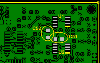
Install U1, U2, C51, and C52
Watch out for solder splashover on any adjacent, open holes
| Designation | Value | Orientation |
|---|---|---|
| C51 | 0.1uF, smt 1206 | smt |
| C52 | 0.1uF, smt 1206 | smt |
| U01 | TLV2462CD op-amp, SOIC 8 | SOIC 8 |
| U02 | TLV2462CD op-amp, SOIC 8 | SOIC 8 |
Testing
Current Draw
- With limiting resistor:
- Without Limiting resistor (should be 34-36 mA ):
Op-Amp Voltage Divider (R15/R16)
- R15/R16 form a voltage divider to halve the 5 Vdc rail
- measure the voltage wrt ground at the R16 hairpin.
- You should see 2.5 Vdc
Op-Amp Pin Voltages
- Measure the voltages at the pins of U1 and U2 using the table below
- You should measure at the actual pins on the ICs as well as using the convenient resistor hairpin testpoints
| Pin | Expected Value | Author Result | As Measured |
|---|---|---|---|
| 1 (R6 hairpin) | 2.5 Vdc | ||
| 2 (R4 hairpin) | 2.5 Vdc | ||
| 3 (R16 hairpin) | 2.5 Vdc | ||
| 4 | 0 (gnd) | ||
| 5 (R16 hairpin) | 2.5 Vdc | ||
| 6 (R7 hairpin) | 2.5 Vdc | ||
| 7 | 2.5 Vdc | ||
| 8 (R15 hairpin) | +5 Vdc |
| Pin | Expected Value | Author Result | As Measured |
|---|---|---|---|
| 1 (R12 hairpin) | 2.5 Vdc | ||
| 2 (R10 hairpin) | 2.5 Vdc | ||
| 3 (R16 hairpin) | 2.5 Vdc | ||
| 4 | 0 (gnd) | ||
| 5 (R16 hairpin) | 2.5 Vdc | ||
| 6 (R13 hairpin) | 2.5 Vdc | ||
| 7 | 2.5 Vdc | ||
| 8 (R15 hairpin) | +5 Vdc |
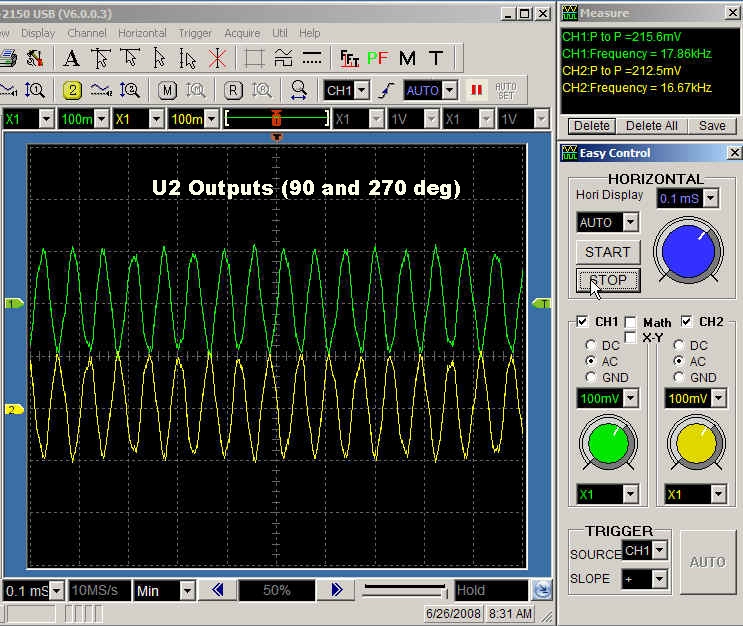
Op-Amp Function
- set up Rocky or IQGen to transmit using a center frequency of 7.056 MHz and transmitting on 7.040 MHz at approximately 215 mV p-p
- connect the board to the PC via a stereo cable to the Line out L and Line Out R (and common) connectors
- clip the scope probes to R5's hairpin (the 0° output of U1) and R8's hairpin (the 180° output of U1)
- You should see equal signals 180° out of phase with one another and at a frequency of approximately 16 kHz
- Repeat the process for U2, using R11 and R14, in lieu of R5 and R8, for the 90° and 270° outputs, respectively