Introduction
This is the final (no pun intended) stage of the build, where the output signal from the Mixer (QSE) stage is amplified and delivered to the antenna. When you gave completed this stage, you are ready to set up the radio for actual transceiving use.There are some tricky maneuvers in this stage, including, but not limited to, the following gotchas:
- Four inductors to wind and install (including the 47 turn L1)
- Some careful bending of the leads of and mounting of Q3, Q5, and Q6
- Installing the heat sinks on the three transistor array and the Q2
- installing some resistors (flat) that must be carefully placed so as not to interfere with the placement of Q2 and its heat sink
Schematic
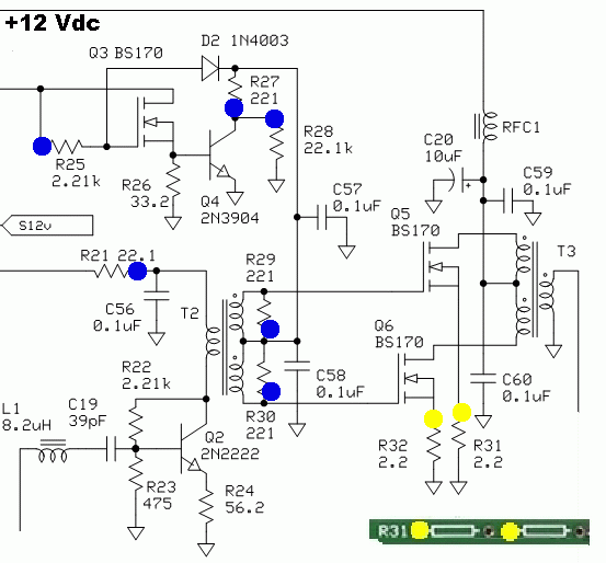
Bill of Materials
| Designation | Value | Orientation |
|---|---|---|
| C19 | 39pF, ceramic, 5% | n/a |
| C20 | 10uF/16 VDC Electrolytic | West-East |
| D2 | 1N4003 | flat |
| hdw | [1] #4 nylon washer mounting hardware for Q2 spacer | |
| hdw | TO18 heat sink Q2 heat sink | |
| hdw | TO220 heat sink Q3, Q5, Q6 heat sink | |
| hdw | 1/2 inch 6-32 phillips pan head machine screw Q3, Q5, Q6 heat sink | |
| hdw | 6-32 hex nut Q3, Q5, Q6 heat sink | |
| hdw | #6 star washer Q3, Q5, Q6 heat sink | |
| hdw | Sil-Pad, TO220 size Q3, Q5, Q6 heat sink | |
| L01 | T30-6 (yellow) (26" #30) (8.2 uH) | 47T |
| Q02 | 2N2222A | TO 18 |
| Q03 | BS170 FET | TO 92 |
| Q04 | 2N3904 NPN | TO 92 |
| Q05 | BS170 FET | TO 92 |
| Q06 | BS170 FET | TO 92 |
| R21 | 1.00 K, 1/4 W, 1% | South-North |
| R22 | 2.21 K, 1/4W, 1% | flat |
| R23 | 475, 1/4 W, 1% | flat |
| R24 | 56.2, 1/4 W, 1% | flat |
| R25 | 2.21 K, 1/4W, 1% | East-West |
| R26 | 33.2, 1/4 W, 1% | South-North |
| R27 | 221, 1/4 W, 1% | North-South |
| R28 | 22.1 K, 1/4W, 1% | South-North |
| R29 | 221, 1/4 W, 1% | West-East |
| R30 | 221, 1/4 W, 1% | West-East |
| R31 | 2.2, 1/4W, 5% | flat |
| R32 | 2.2, 1/4W, 5% | flat |
| RFC1 | BN-43-2402 (5" #26) | 4T |
| T02 | BN-43-2402 (10"/2x4.5" #30) | 6T/2x3T |
| T03 | BN-43-2402 (10"/2x6" #30) | 5T/2x4T |
Build Notes
Resistors (12) and Diode D2
- mount the resistors first
- take care when mounting R22, R23, and R24 (leave room for Q2's heatsink
- Mount D2
Capacitors (2)
- mount the capacitors C19 and C20
Inductors
Turn counts: remember that, for a toroid core, each pass through the center counts as a turn. For a binocular core, each pass where the wire ends up at the same side where it started the pass counts as a turn- L1 (T30-6, yellow toroid): wind and mount L1 (47 turns = 26" #30)
- You may encounter problems trying to fit 47 turns of #30 wire onto the T30-6 Toroid. DL5SWB’s Mini-Ring Calculator program specifies #31 wire is the max size wire to get the 47 turns required.
- Most winders have run out of space at around 38 turns, distributing the remaining 9 turns over the top of the preceding 38 turns.
- It may be possible to go to a T37-6 core and use 52 turns of #30.
- T2 (binocular): Wind and mount T2 (Primary: 6 turns = 10" #30; Secondaries: 3 turns bifilar = 2 x 5" #30).
- (A small sewing needle has been proven to be a great aid in winding these binocular cores, however, you should take great care to keep the needle from removing any insulation on the wires in the windings
Transistors Q4 and Q2
- Mount transistor Q4 (2N3904)
- Driver transistor Q2 (2N2222A) may be mounted after T2 is properly mounted.
- Press the TO-18 heat sink onto Q2 by placing the top of the heat sink (the wide, flat “hat”) on a hard flat surface and then pressing uniformly on the lower rim of the transistor to fully insert it into the heat sink.
- A #4 nylon washer is included in the kit as a spacer between the bottom of the transistor
and the circuit board.
- Slip the leads of the transistor through the nylon washer’s hole
- Snug the transistor to the circuit board.
- Exercise care to make sure the emitter lead of Q2 by the metal tab on the transistor case goes to the hole closest to the silkscreen emitter mark on the circuit board.
Inductors
- T3 (binocular): Wind and Mount T3 (Secondary: 5 turns = 9" #30; Primaries 4 turns bifilar = 2x6" #30 )
- RFC1 (binocular): Wind and Mount RFC1 (4 turns = 5" #26)
Transistor/Heatsink Stack
- Transistors Q3, Q5 and Q6 are mounted with their flat side facing upward so that
the entire flat side of each transistor will be under an aluminum TO220 heat sink.
- Bend the leads of Q3, Q5 and Q6 at right angles away from the flat side of each transistor at a distance from the plastic body of each transistor so that its case end is very close to the heat sink mounting hole in the board.
- When a transistor is properly placed solder one of its leads from the top side of the board to tack the transistor in position.
- After Q3, Q5 and Q6 are tacked in place with their flat sides facing upward, mount the heat sink with the Sil-Pad between the flat sides of the transistors and the bottom surface of the heat sink.
- The heat sink stack up should be as follows: from the bottom of the circuit
board:
- the ½ inch long 6-32 Phillips machine screw,
- the circuit board,
- the transistors with flat faces upward,
- the TO220 Sil-Pad,
- the TO220 heat sink with fins upward,
- he #6 star washer,
- and the 6-32 hex nut.
- Tighten the 6-32 hardware carefully to firmly compress the stack while holding the heat sink in alignment with the rectangular markings on the circuit board. Be careful that the tightening of the #6 hardware does not cause a twisting motion of the transistors.
- When the transistors are firmly clamped between the board and heat sink with good alignment, complete the soldering of the transistor leads and trim the lead flush to the bottom of the board.
Testing
Power Rail Resistances
- +5Vdc testpoint should be ~810 ohms WRT ground
- +12 V testpoint should be very high (> 100 k Ohm) WRT ground
Current Draw (Power drain s/b ~444 mW)
- With limiting resistor.
- without limiting resistor you should see < 50 mA (approximately 38 mA)
PTT Current Draw
PTT input function may be verified by connecting PTT input line, (I PTT), to 12 volts. (Exercise care in connecting 12 volts to the PTT input line because a connection of 12 volts to the PTT output line, (PTT O), can damage U3.)- Cliplead connect R33 hairpin to R35 hairpin (forces I-PTT to high)
- Measure current draw (should be less than 160 mA (1.92 W)). You should see __________
RFC1 Continuity
- measure the voltage at the top end of RFC1 (expect 12 Vdc)
- measure the voltage at the bottom end of RFC1 (expect 12 Vdc)
PA Standing Current
PA standing current is checked by connecting PTT-in to 12 volts and measuring the voltage across resistors R31 and R32. The DC voltage across each resistor should be 55 mVDC +/- 10mVDC.- Cliplead connect R33 hairpin to R35 hairpin (forces I-PTT to high)
- Measure the dc voltage across R31 (s/b ~55 mVdc +/- 10 mVdc)
- Measure the dc voltage across R32 (s/b ~55 mVdc +/- 10 mVdc)
Miscellaneous Voltage Tests
The test measurements outlined here (all with PTT-I high) may aid in trouble-shooting your board.
| Measured at | Expected Value (Vdc) | Measured As |
|---|---|---|
| R21 hairpin (T2 pri) | ~the 12 V rail | |
| R25 hairpin | ~the 12 V rail | |
| R26 hairpin | 0.7 | |
| R27 hairpin | 1.8 | |
| R29 hairpin | 2.5 | |
| R30 hairpin | 2.5 | |
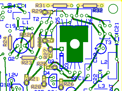
| Q5 Drain (see bottomside view above) | ~the 12 V rail | |
| Q6 Drain (see bottomside view above) | ~the 12 V rail | |
| Each Primary lead on T3 (see bottomside view above) | ~the 12 V rail | |
| Each Secondary lead on T2 (see bottomside view above) | 2.5 |
This area is notorious for bad solder joints. If your results are not as expected, check/touch up the solder joints on the transformers and MOSFETs.
RF Output
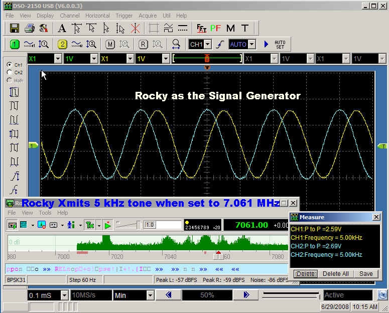
A quadrature audio source can be used for initial testing of the transmit function. Quadrature audio can be provided from a PC soundcard line-out if a program such as IQ GEN by DL6IAK or Rocky is installed on the PC.Note: on the author's PC, IQ Gen was unable to produce the required 2.4 V p-p signals needed to drive the transmitter to its full 1 W output. However, it still serves as a means to produce an adjustable level of I and Q signals for initial tests.
TX Input Test
(Usual caveats as to author's scope's accuracy and stability apply here)- Connect the antenna coax cable from the circuit board to a 50 ohm load.
- Setup Rocky for your desired center frequency (here, we're using 7.056 MHz)
- Tune Rocky's spectrum view to the desired frequency approximately 5 kHz up or down from the center frequency (here, we're using 7.061 MHz)
- Power up the board and connect I PTT to 12 Vdc (clip R33 to R35)
- Connect the soundcard's Line Out to the "Line Out" pads on the board
- Measure the p-p voltage at the LineOut pads. You should see 2.4-2.6 V p-p
- check for RF output across the 50 ohm load as the quadrature audio level is increased from the IQ GEN amplitude slider
- If your PC cannot push IQ Gen out to 2.4 V p-p levels, set up Rocky to transmit (i.e., send out I and Q signals) Set the center frequency of Rocky accordingly and select a frequency on the spectrum display approximately 5 kHz above or below the center frequency. Click on the "TX" button at the top of the screen, select "Tone" to get a single sine wave out of the PC's sound card..
- The RF voltage across the 50 ohm load should go to 20V p-p, (1 watt output), when the quadrature audio inputs are each at 2.4V p-p.
- The RF output waveform across the 50 ohm load should appear as a clean looking sine wave when viewed with a scope. The frequency of the RF voltage should be equal to the center frequency + or - 5 kHz where the + or - frequency offset depends on the line-out signal phase relationship between the two line-out channels.
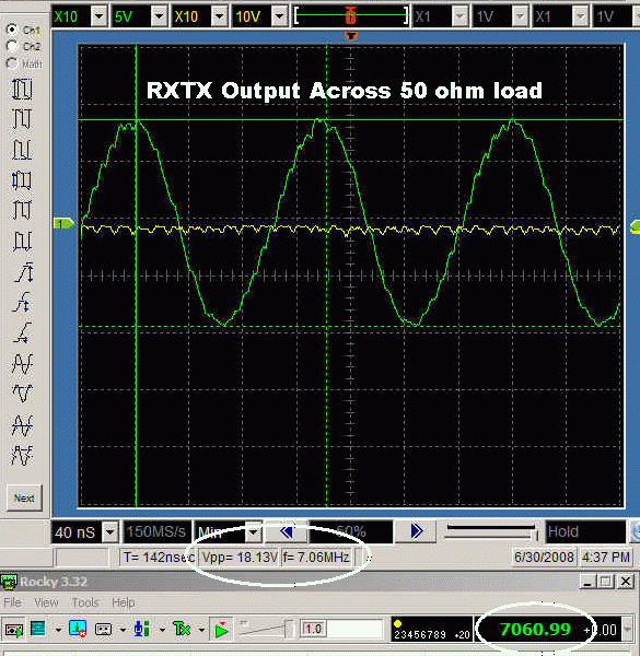
PA Output Test
(Usual caveats as to author's scope's accuracy and stability apply here)- Use the same Rocky setup from above
- Connect your antenna terminals to a 50 ohm load
- check for RF output across the 50 ohm load as Rocky's "IQ Volume" audio level is increased towards max
- The RF voltage across the 50 ohm load should go to ~20V p-p, (1 watt output), when the quadrature audio inputs are each at 2.4V p-p.
- The RF output waveform across the 50 ohm load should appear as a clean looking sine wave when viewed with a scope. The frequency of the RF voltage should be equal to the center frequency + or - 5 kHz where the + or - frequency offset depends on the line-out signal phase relationship between the two line-out channels.
- The example shown below has the correct wave form and frequency, but the V p-p is a little on the low side (however this may well be due to the calibration and accuracy of the author's cheapo scope).
- If you do not get the RF voltage levels specified above, see message #26506 on the Softrock reflector concerning changes that can be made to reduce R3 and R9 from 10k to 4.99k (to increase the gain of the TX OpAmps in the TX Opamps Stage)
- The power output is derived using the following formula:
[ (Vpk)2 * 0.125 ] / 50
= [ (18.13)2 * 0.125 ] / 50
= 0.82 W (820 mW)
TX I/Q Balancing
Balance the I and Q outputs of Rocky (phase and gain) for the cleanest image rejection during transmit.
While not actually a "test procedure", the process of TX I/Q Balancing is a last step to enabling a fully functional, optimized TX for the RXTX V6.2 (this applies to use of the RXTX V6.2 with the Rocky software).