Busses and Rails Introduction
General
This stage provides the infrastructure "backbone" needed to support the switches and band filter chains.
(go directly to build notes)Busses and Rails Schematic
(Resistor testpoints (hairpin, top, or left-hand lead), as physically installed on the board, are marked in the schematic with red dots)
(Click for Full Schematic)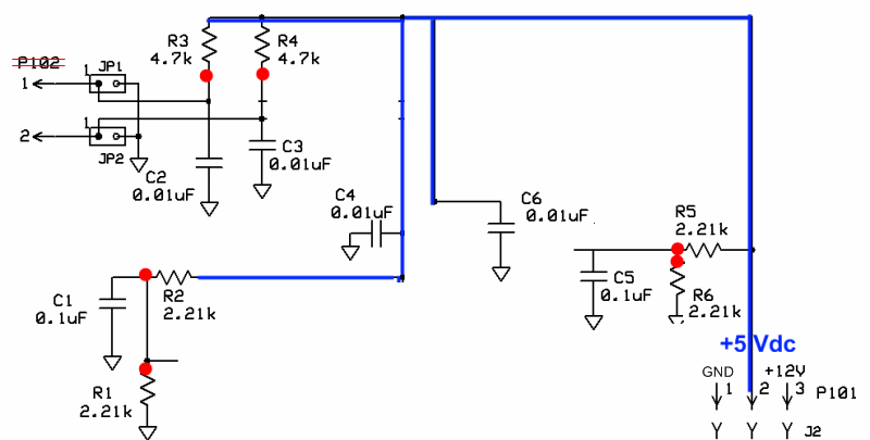 (go directly to build notes)
Busses and Rails Bill of Materials
Stage Bill of Materials
(resistor images and color codes courtesy of WIlfried, DL5SWB's R-Color Code program)
| Check | Designation | Component | Marking | Category | Orientation | Notes | Circuit |
|---|---|---|---|---|---|---|---|
| ❏ | C06 | 0.01 uF | (smt)
 | SMT 1206 | Busses and Rails | ||
| ❏ | C01 | 0.1 uF | (smt) black stripe
 | SMT 1206 | Busses and Rails | ||
| ❏ | JP1 | header, 2-pin w/jumper |
 | Jumper | Busses and Rails | ||
| ❏ | R01 | 2.21 k 1/4W 1% | r-r-br-br-br
 | 1/4W | E-W | Busses and Rails | |
| ❏ | C02 | 0.01 uF | (smt)
| SMT 1206 | Busses and Rails | ||
| ❏ | C19 | 0.01 uF | (smt)
| SMT 1206 | Busses and Rails | ||
| ❏ | JP2 | header, 2-pin w/jumper |
| Jumper | Busses and Rails | ||
| ❏ | R02 | 2.21 k 1/4W 1% | r-r-br-br-br
| 1/4W | W-E | Busses and Rails | |
| ❏ | C03 | 0.01 uF | (smt)
| SMT 1206 | Busses and Rails | ||
| ❏ | P100 | header, 9-pin |
 | Header | Busses and Rails | ||
| ❏ | R03 | 4.7 k 1/4 W 5% | y-v-r-gld
 | 1/4W | W-E | Busses and Rails | |
| ❏ | C04 | 0.01 uF | (smt)
| SMT 1206 | Busses and Rails | ||
| ❏ | P101 | header, 3-pin |
 | Header | Pins: 1=gnd; 2=+5 Vdc; 3=+12Vdc. From V9.0 J2 | Busses and Rails | |
| ❏ | R04 | 4.7 k 1/4 W 5% | y-v-r-gld
| 1/4W | W-E | Busses and Rails | |
| ❏ | C05 | 0.1 uF | (smt) black stripe
| SMT 1206 | Busses and Rails | ||
| ❏ | R05 | 2.21 k 1/4W 1% | r-r-br-br-br
| 1/4W | W-E | Busses and Rails | |
| ❏ | R06 | 2.21 k 1/4W 1% | r-r-br-br-br
| 1/4W | E-W | Busses and Rails |
Busses and Rails Summary Build Notes
- Install Bottomside SMT Caps
- Install Topside SMT Caps
- Install Resistors
- Install Connectors
- Test the Stage
Busses and Rails Detailed Build Notes
Bottom of the Board
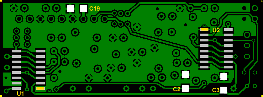
Install Bottomside SMT Caps
See graphic above: pads for 0.01 uF caps are white
| Check | Designation | Component | Marking | Category | Orientation | Notes |
|---|---|---|---|---|---|---|
| ❏ | C02 | 0.01 uF | (smt)
| SMT 1206 | ||
| ❏ | C19 | 0.01 uF | (smt)
| SMT 1206 | ||
| ❏ | C03 | 0.01 uF | (smt)
| SMT 1206 |
Top of the Board
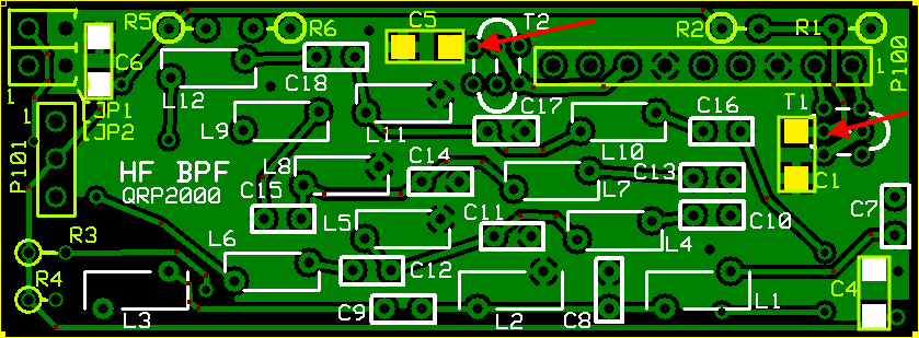
Install Topside SMT Caps
See graphic above: pads for 0.01 uF caps are white
Take great care in soldering C5 and C1 to the board. The right-hand end of C5 and the top end of C1 are very close to thru-holes for T2 and T1 (see red arrows on the topside board view), respectively. You do NOT want to inadvertently splash solder into these holes (transformer mounting is hard enough without having to deal with solder residue blocking the holes).
The author used a fine-pointed, wooden toothpick to block the holes when soldering these caps.
| Check | Designation | Component | Marking | Category | Orientation | Notes |
|---|---|---|---|---|---|---|
| ❏ | C06 | 0.01 uF | (smt)
| SMT 1206 | ||
| ❏ | C01 | 0.1 uF | (smt) black stripe
| SMT 1206 | ||
| ❏ | C04 | 0.01 uF | (smt)
| SMT 1206 | ||
| ❏ | C05 | 0.1 uF | (smt) black stripe
| SMT 1206 |
Install Resistors
Resistor Orientation Codes
Note the orientation ("NS" means the resistor barrel is in the "northern" hole and the hairpin lead is in the "southern" hole. Orientation codes "WE", "EW", and "SN" operate in a similar fashion
| Check | Designation | Component | Marking | Category | Orientation | Notes |
|---|---|---|---|---|---|---|
| ❏ | R01 | 2.21 k 1/4W 1% | r-r-br-br-br
| 1/4W | E-W | |
| ❏ | R02 | 2.21 k 1/4W 1% | r-r-br-br-br
| 1/4W | W-E | |
| ❏ | R03 | 4.7 k 1/4 W 5% | y-v-r-gld
| 1/4W | W-E | |
| ❏ | R04 | 4.7 k 1/4 W 5% | y-v-r-gld
| 1/4W | W-E | |
| ❏ | R05 | 2.21 k 1/4W 1% | r-r-br-br-br
| 1/4W | W-E | |
| ❏ | R06 | 2.21 k 1/4W 1% | r-r-br-br-br
| 1/4W | E-W |
Install Connectors
- JP1 & 2 installed to board top, with Pins pointing upwards
- P100 & 101 installed to bottom of board, with pins pointing downward (so as to ultimately mate with the V9.0 board)
- Once the firmware for the V9.0 RX is rewritten to provide the control signals for the BPF switching, JP1 and JP2 will be connected via a cable to the (male) J3 on the V9.0 RX board
| Check | Designation | Component | Marking | Category | Orientation | Notes |
|---|---|---|---|---|---|---|
| ❏ | JP1 | header, 2-pin w/jumper |
| Jumper | ||
| ❏ | JP2 | header, 2-pin w/jumper |
| Jumper | ||
| ❏ | P100 | header, 9-pin |
| Header | ||
| ❏ | P101 | header, 3-pin |
| Header | Pins: 1=gnd; 2=+5 Vdc; 3=+12Vdc. From V9.0 J2 |
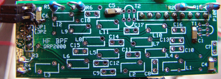
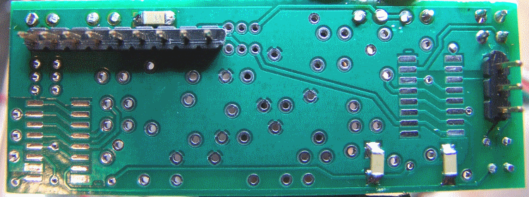
Busses and Rails Completed Stage
Top of the Board
Bottom of the Board
Busses and Rails Testing
Visual Check
Test Setup
Using very good lighting and magnification, carefully inspect the solder joints to identify bridges, cold joints, or poor contacts.
Resistance Tests
Test Setup
The following tests help validate there is are good solder joints and no shorts on the power rail and should be passed before applying power to the HF-BPF board. If these tests are passed, you can be pretty sure the voltage tests will succeed.
Test Measurements
| Testpoint | Units | Nominal Value | Author's | Yours |
|---|---|---|---|---|
| P101-pin 2 to P100 pin 3 | k ohms | 2.21 | 2.21 | _______ |
| Right-hand pin of JP1 to P100 pin 3 | ohms | 0 | 0 | _______ |
| Right-hand pin of JP2 to P100 pin 3 | ohms | 0 | 0 | _______ |
| R4 hairpin to P101 pin 2 | k ohms | 4.7 | 4.72 | _______ |
| R3 hairpin to P101 pin 2 | k ohms | 4.7 | 4.63 | _______ |
| JP1 left-hand pin to P101 pin 2 | k ohms | 4.7 | 4.63 | _______ |
| JP2 left-hand pin to P101 pin 2 | k ohms | 4.7 | 4.72 | _______ |
| C5 right-hand end to P101 pin 2 | k ohms | 1.7 | 1.64 | _______ |
| C1 top end to P101 pin 2 | k ohms | 1.7 | 1.65 | _______ |
VoltageTests
Test Setup
This test assumes you have a V9.0 Lite + Xtall RX board that has been completed through (at least) the power supply stage. This is required because you want to test the "fit" of P100 and P101 to their corresponding jacks (J1 and J2) on the RX board and the RX board is a convenit=ent source of regulated 5 Vdc power.
- Test the installation of P100 and P101 for "fit" by plugging the HF-BPF board into J1 and J3 of the V9.0 RX board
- Make sure JP1 and JP2 are un-jumpered. This should ensure that R3 abd R4 cause Pins 1 of JP1 and JP2 to be pulled up to the 5 volt rail.
- Apply power (9-12 Vdc) to the V9.0 RX board
- Measure the voltages with respect to ground according to the table below (you can use either of the right-hand pins on JP1 or JP2 as a convenient ground connection)
Test Measurements
| Testpoint | Units | Nominal Value | Author's | Yours |
|---|---|---|---|---|
| P101-Pin2 | Vdc | 5 | 4.96 | _______ |
| R6, hairpin lead | Vdc | 2.5 | 2.48 | _______ |
| R1, hairpin lead | Vdc | 2.5 | 2.48 | _______ |
| R3, hairpin lead | Vdc | 5 | 2.96 | _______ |
| R4, hairpin lead | Vdc | 5 | 4.96 | _______ |