Operational Amplifiers Introduction
General
The operational amplifiers take, as input, the output of the QSD stage and amplify the it to pass it through as I and Q signals to the output pins.
Band-Specific Components
Some of the components in this phase are band-specific. The Bills of Material below specify the common components and the 40m-specific components. If you are building another band's kit, you should refer to the following chart for their component values:
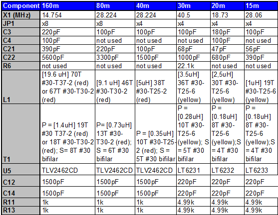
Note that for the 30m and up bands, the QSD uses 1/3 sub-harmonic sampling. This results in the I and Q being reversed. So the builder should, when connecting the rig, wire the I/Q cable to reflect this fact.
(go directly to build notes)Operational Amplifiers Schematic
(Resistor testpoints (hairpin, top, or left-hand lead), as physically installed on the board, are marked in the schematic with red dots)
(Click for Full Schematic)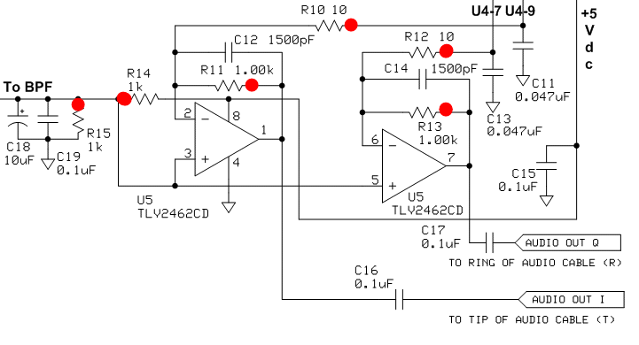
(go directly to build notes)
Operational Amplifiers Bill of Materials
Stage Bill of Materials
(resistor images and color codes courtesy of WIlfried, DL5SWB's R-Color Code program)
| Check | Designation | Component | Marking | Category | Orientation | Notes | Circuit |
|---|---|---|---|---|---|---|---|
| ❏ | U5 | TLV2462CD dual opamp | TVL2462CD
 | SOIC-8 | LT6231 for 30m, 20m, 15m | Operational Amplifiers | |
| ❏ | C15 | 0.1 uF | (smt) black stripe
 | SMT 1206 | Operational Amplifiers | ||
| ❏ | C16 | 0.1 uF | (smt) black stripe
 | SMT 1206 | Operational Amplifiers | ||
| ❏ | C17 | 0.1 uF | (smt) black stripe
 | SMT 1206 | Operational Amplifiers | ||
| ❏ | C19 | 0.1 uF | (smt) black stripe
 | SMT 1206 | Operational Amplifiers | ||
| ❏ | C11 | 0.047 uF 5% | 473
 | Ceramic | Operational Amplifiers | ||
| ❏ | C12 | 1500 pF 10% | 152
 | Ceramic | 220pF for 30m, 20m, 15m | Operational Amplifiers | |
| ❏ | C13 | 0.047 uF 5% | 473
 | Ceramic | Operational Amplifiers | ||
| ❏ | C14 | 1500 pF 10% | 152
 | Ceramic | 220pF for 30m, 20m, 15m | Operational Amplifiers | |
| ❏ | C18 | 10uF/16 VDC |
 | Electrolytic | Operational Amplifiers | ||
| ❏ | R10 | 10 ohm 1/4W 1% | br-blk-blk-gld-br
 | 1/4W | W-E | Operational Amplifiers | |
| ❏ | R11 | 1 k 1/4W 1% | br-blk-blk-br-br
 | 1/4W | E-W | 4.99k for 30m, 20m, 15m | Operational Amplifiers |
| ❏ | R12 | 10 ohm 1/4W 1% | br-blk-blk-gld-br
 | 1/4W | S-N | Operational Amplifiers | |
| ❏ | R13 | 1 k 1/4W 1% | br-blk-blk-br-br
 | 1/4W | E-W | 4.99k for 30m, 20m, 15m | Operational Amplifiers |
| ❏ | R14 | 1 k 1/4W 1% | br-blk-blk-br-br
 | 1/4W | W-E | Operational Amplifiers | |
| ❏ | R15 | 1 k 1/4W 1% | br-blk-blk-br-br
 | 1/4W | W-E | Operational Amplifiers |
Operational Amplifiers Summary Build Notes
- Install U5, Dual OpAmp
- Install SMT Caps
- Install Topside SMT Cap
- Install Ceramic Caps
- Install Electrolytic Cap
- Install Resistors
- Test the Stage
Operational Amplifiers Detailed Build Notes
Bottom of the Board
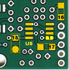
Install U5, Dual OpAmp
U5 is either a TLV2462 (for the 160m, 80m, and 40m) kits or a LT6231 (for the 30m, 20m, 15m kits).
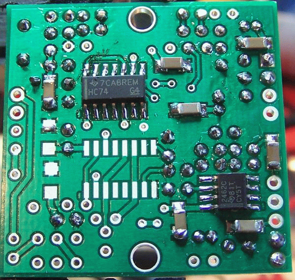
Orient U5 on its pads so that the pin 1 corner of the IC matches the small �1" (it also looks like a �0�) mark in the copper on the bottom side of the board. In general, pin 1 of an SOIC packaged IC is in the lower left corner of the package when the printing on the package top reads upright, from left to right.
Tack-solder one corner pin of U5 and reheat the tacked pin as necessary to line up U5 on its pads properly.
Double-check the orientation of U5 and the line up of the IC on its pads with magnification and good lighting. You do NOT want to install U5 oriented incorrectly. If all is well, carefully solder the rest of the leads to their pads.
| Check | Designation | Component | Marking | Category | Orientation | Notes |
|---|---|---|---|---|---|---|
| ❏ | U5 | TLV2462CD dual opamp | TVL2462CD
 | SOIC-8 | Take ESD precautions LT6231 for 30m, 20m, 15m |
Install SMT Caps
| Check | Designation | Component | Marking | Category | Orientation | Notes |
|---|---|---|---|---|---|---|
| ❏ | C15 | 0.1 uF | (smt) black stripe
 | SMT 1206 | ||
| ❏ | C16 | 0.1 uF | (smt) black stripe
 | SMT 1206 | ||
| ❏ | C17 | 0.1 uF | (smt) black stripe
 | SMT 1206 |
Top of the Board
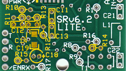
Install Topside SMT Cap
| Check | Designation | Component | Marking | Category | Orientation | Notes |
|---|---|---|---|---|---|---|
| ❏ | C19 | 0.1 uF | (smt) black stripe
 | SMT 1206 |
Install Ceramic Caps
| Check | Designation | Component | Marking | Category | Orientation | Notes |
|---|---|---|---|---|---|---|
| ❏ | C11 | 0.047 uF 5% | 473
 | Ceramic | ||
| ❏ | C12 | 1500 pF 10% | 152
 | Ceramic | 220pF for 30m, 20m, 15m | |
| ❏ | C13 | 0.047 uF 5% | 473
 | Ceramic | ||
| ❏ | C14 | 1500 pF 10% | 152
 | Ceramic | 220pF for 30m, 20m, 15m |
Install Electrolytic Cap
C18 is installed with attention paid to ensuring the positive lead (the longest lead) goes to the positive (�+�) hole.
| Check | Designation | Component | Marking | Category | Orientation | Notes |
|---|---|---|---|---|---|---|
| ❏ | C18 | 10uF/16 VDC |
 | Electrolytic |
Install Resistors
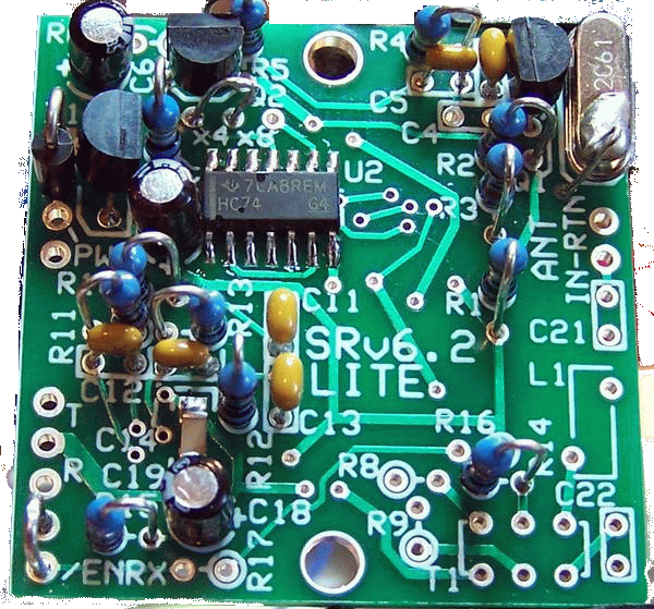
Finally, install the five resistors (R10-R14) on the top side of the board. Note that R14 and R16 could be confused: R14 lies below R16:
Note also that R11 and R13 are band-specific (1k for the 160m, 80m, 40m kits and 4.99k for the 160m, 80m, and 40m kits)
| Check | Designation | Component | Marking | Category | Orientation | Notes |
|---|---|---|---|---|---|---|
| ❏ | R10 | 10 ohm 1/4W 1% | br-blk-blk-gld-br
 | 1/4W | W-E | |
| ❏ | R11 | 1 k 1/4W 1% | br-blk-blk-br-br
 | 1/4W | E-W | 4.99k for 30m, 20m, 15m |
| ❏ | R12 | 10 ohm 1/4W 1% | br-blk-blk-gld-br
 | 1/4W | S-N | |
| ❏ | R13 | 1 k 1/4W 1% | br-blk-blk-br-br
 | 1/4W | E-W | 4.99k for 30m, 20m, 15m |
| ❏ | R14 | 1 k 1/4W 1% | br-blk-blk-br-br
 | 1/4W | W-E | |
| ❏ | R15 | 1 k 1/4W 1% | br-blk-blk-br-br
 | 1/4W | W-E |
Operational Amplifiers Completed Stage
Top of the Board
Bottom of the Board
Operational Amplifiers Testing
Warning
Test Setup
Take appropriate ESD precautions in these tests, since you will be working around the sensitive OpAmp IC
Visual Inspection
Test Setup
Using very good lighting and magnification, carefully inspect the solder joints to identify bridges, cold joints, or poor contacts.
Pay especial attention to the joints on the OpAmp IC pins. If necessary, touch up the joints with your iron and/or some flux. Wick up any excess.
Current Draw
Test Setup
- connect a 1k ohm resistor in series with the positive power lead
- apply 9 Vdc and measure the current draw with the limiting resistor in place
- remove the current limiting resistor
- apply 9 Vdc and measure the current draw without the limiting resistor
Test Measurements
| Testpoint | Units | Nominal Value | Author's | Yours |
|---|---|---|---|---|
| Current draw WITH 1k ohm current limiting resistor | mA | < 9 | 6.1 | _______ |
| Current draw without the limiting resistor | mA | 25-35 | 28.1 | _______ |
IC Pin Voltages
Test Setup
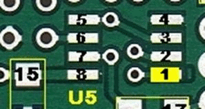
In addition to using the convenient test points indicated in the table below, you should also double check by measuring the voltages on the actual IC pins (to detect the case of a poor or missing solder joint between the pin and the pad.
expected voltages are indicated in the table below:
- 5 V (range of 4.5 - 5.4)
- 2.5 V (approx 50% of the 5B rail value)
Test Measurements
| Testpoint | Units | Nominal Value | Author's | Yours |
|---|---|---|---|---|
| pin 1 | Vdc | 2.5 | 2.48 | _______ |
| pin 2 | Vdc | 2.5 | 2.48 | _______ |
| pin 3 | Vdc | 2.5 | 2.48 | _______ |
| pin 4 | Vdc | 0 | 0 | _______ |
| pin 5 | Vdc | 2.5 | 2.48 | _______ |
| pin 6 | Vdc | 2.5 | 2.48 | _______ |
| pin 7 | Vdc | 2.5 | 2.48 | _______ |
| pin 8 | Vdc | 5 | 4.94 | _______ |
Op Amp Function Test
Test Setup
You will test the DC gain of each of the op-amps by connecting bridging resistors RB from each op-amp inverting input to circuit ground. Introducing the "bridging" resistor RB will result in a test current equal to 2.5 / Rt which will be balanced by the current fed back from each op-amp's output through each feedback resistor, RF (i.e., R11 or R13). Each op-amp output will increase in voltage by 2.5 * RF/ RB from the nominal DC level of 2.5 volts.
The value of the "bridging" resistor (RB) will depend upon the OpAmp used in the circuit:
- RB=2.2 kΩ for the TLV2462 (160m, 80m, or 40m kit)
- RB=10 kΩ for the LT6231 (30m, 20m, or 15m kit)
Test the First OpAmp
Power up the circuit and measure the voltage at pin 1 of the op-amp (hairpin of R11). It should be ~2.5 Vdc- Power off and use clip leads to connect RB between the hairpin of R10 and circuit ground. (This provides an input resistance(Ri) of 2.2 k(+10)Ω or 10 k (+10)Ω (depending on the band) to the op-amp).
- Power up and measure the output voltage at the hairpin of the feedback resistor R11. You should get:
- For the TLV2462, with RB = 2.210 kΩ and R11 = 1.010 kΩ: ~3.6 Vdc
- For the LT6231, with RB=10 kΩ and R11=5 kΩ: ~3.75 Vdc.
- Remove RB and the output voltage at R11 should go back to ~2.5 Vdc.
Test the Second OpAmp
Power up the circuit and measure the voltage at pin 7 of the op-amp (hairpin of R13). It should be ~2.5 Vdc- Power off and use clip leads to connect RB between the hairpin of R12 and circuit ground. (This provides an input resistance(Ri) of 2.210 kΩ or 10.010 kΩ (depending on the band) to the op-amp).
- Power up and measure the output voltage at the hairpin of the feedback resistor R13. You should get:
- For the TLV2462, with RB = 2.21 kΩ and R12 = 1.01 kΩ: ~3.6 Vdc
- For the LT6231, with RB=10 kΩ and R12=5 kΩ: ~3.75 Vdc.
- Remove RB and the output voltage at R7 should go back to ~2.5 Vdc.
An Excel spreadsheet with a calculator for this test is available for you to plug in your bridging resistor ohms (Rt) and your pin 1 or pin 7 normal voltages (Ebias) and predict the expected voltage when bridged (Eout).
Test Measurements
| Testpoint | Units | Nominal Value | Author's | Yours |
|---|---|---|---|---|
| Normal pin 1 (R1 not connected) | Vdc | 2.4 - 2.5 | 2.5 | _______ |
| normal pin 7 | Vdc | 2.4 - 2.5 | 2.5 | _______ |
| (160/80/40m kit) pin 1 bridged with 2.2k resistor | Vdc | ~3.6 | 3.63 | _______ |
| (160/80/40m kit) pin 7 bridged with 2.2k resistor | Vdc | ~3.6 | 3.63 | _______ |
| (30/20/15m kit) pin 1 bridged with 10k resistor | Vdc | ~3.75 | n/a | _______ |
| (30/20/15m kit) pin 7 bridged with 10k resistor | Vdc | ~3.75 | n/a | _______ |